-
Welcome to Overclockers Forums! Join us to reply in threads, receive reduced ads, and to customize your site experience!
You are using an out of date browser. It may not display this or other websites correctly.
You should upgrade or use an alternative browser.
You should upgrade or use an alternative browser.
Nvidia to pay out for class action for 970 vram fiasco
- Thread starter Janus67
- Start date
- Joined
- Jun 7, 2011
 Oh dear, i had a good laught, thanks.
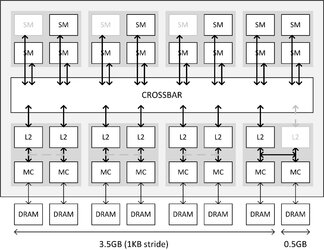
Performance = speed.The difference isn't in speed. ALL 4GB run at the same speed using the same bus width. The problem was with one (of four) partially disabled ROPs/Memory Controller. It has 56 ROPS and 1.75MB of L2 cache. Here is an article that should prove to be pretty informative: http://www.anandtech.com/show/8935/geforce-gtx-970-correcting-the-specs-exploring-memory-allocation
Well, I am sure you meant speed a bit more nebulous than I did, lol!
The biggest impact of this configuration is that it creates the segmented memory conditions NVIDIA outlined in their earlier statement. Due to performance issues from the unbalanced ROP/MC partition, NVIDIA segments the memory into a high-performance 3.5GB segment – what they refer to as segment 0 – and a low-performance 512MB (0.5GB) segment containing the rest of the RAM. It is this segmentation that results in some of the previously-unusual memory allocation behaviors and memory bandwidth benchmarks on the GTX 970. http://www.anandtech.com/show/8935/...cting-the-specs-exploring-memory-allocation/2
ED, we're giving you sass because nvidia promised "A" but delivered "B". You are defending them for some god-only-knows reason that we just dont understand. Either you're playing devil's advocate here, or to be frank, you're telling people they are "wrong" for wanting what they actually paid for (regardless of impact or not).
It's hopeless...
All I wanted to do was shed some light on why it's actually happening. People think it's 128 bit or runs slower (as in mhz)... but that wasn't the problem. So I replied with anand's article to clarify....
...and here we are.
In other words, I took ivy's "speed" as mhz and replied to clarify the source of the issue. Yes...I'm too literal!
Better? Can we move on?
Last edited:
EarthDog I think the GHz decrease in speed is worse.

This in turn is why the 224GB/sec memory bandwidth number for the GTX 970 is technically correct and yet still not entirely useful as we move past the memory controllers, as it is not possible to actually get that much bandwidth at once when doing a pure read or a pure write. In the case of pure reads for example, GTX 970 can read the 3.5GB segment at 196GB/sec (7GHz * 7 ports * 32-bits), or it can read the 512MB segment at 28GB/sec, but it cannot read from both at once; it is a true XOR situation. The same is also true for writes, as only one segment can be written to at a time. http://www.anandtech.com/show/8935/...cting-the-specs-exploring-memory-allocation/2

- Joined
- Sep 25, 2015
I just received my $30.00 check from Nvidia, Sweet.Did anyone else get theirs?
So THAT'S why they released the Titan X Ppppp
I just received my $30.00 check from Nvidia, Sweet.Did anyone else get theirs?
No, and I signed up last year. I figured they decided they werent going to pay out and someone would have to sue them again. lol
Last edited:
- Joined
- Jun 30, 2004
- Location
- San Antonio, Texas
got my check today
got my check today
That took a long time.
- Joined
- Jun 30, 2004
- Location
- San Antonio, Texas
yeah I was beginning to wonder about it lol
That took a long time.
Not as long as never, which is where I am at.
Not as long as never, which is where I am at.
How come you are denied the payout?
How come you are denied the payout?
I wasent denied anything, I just never received a check. I went to the website, filled out all the info with my mailing address and... Nothing. Of course there doesent seem to be anyway to follow up with it either. No one to contact.
Similar threads
- Replies
- 6
- Views
- 443

