- Joined
- Apr 1, 2002
A recent search brought me to the timeless running Tualatin on CuMine MB w/o Powerleap thread and I decided it was time to dig up some of my classic hardware and show some of the newer members what overclocking was like last century.
But first a bit of history:
Back when companies like Asus and Abit would defy intel and build boards to run CPUs in all sorts of unsupported configurations, when FSB or Vcore changes were made by jumpers or soldering iron, when motherboard manuals were so badly translated they were hilariously frustrating to read, when there were only 12 different types of Lego pieces, and yes, when you had to walk 20 miles to school each day - uphill both ways...
The 16bit 8086 (1978) gave birth to the x86 architecture. The 8088 was a more cost effective variant with an 8bit external bus. If you needed hardware floating point capability (ie: for AutoCad) you'd have to add the 8087 coprocessor.
As a tribute to the 8086, Intel's PCI Vendor ID is 8086.
The 80186 was used mainly for embedded applications.
The 286 (1982) improved the 8086.
The 32bit 386 (1985) was a huge leap in performance and features, and allowed you to multitask using Windows 3.1.
The 486 (1989) integrated the floating point coprocessor into the CPU resulting in a huge increase in floating point ops. AutoCAD users wept with joy.
The P5 / Pentium (1993) continued the evolution of the x86 family adding the capability to execute more then one instruction per clock, and eventually introduced the MMX instruction set. These CPUs were paired with 430 series chipsets.
Which brings us to the age where this build originates - the P6 era. The P6 family originated in 1995 and lasted until Netburst made it's debut in 2000. Due to its high efficiency in 2003 an enhanced version of the P6 architecture was revived as the "Core" series (Pentium M) which was eventually succeeded by the 64bit "Core 2" series in 2006.
The first P6 CPU was the Pentium Pro (1995). One of the main features was the on-package L2 cache which was connected via a BSB (Back Side Bus) and ran at full CPU speed. Because this on-package L2 arrangement was difficult to manufacture yields were low and the cost of the Pentium Pro CPUs was high.
Unable to bring on-package L2 yields under control, in 1997 the Pentium II was introduced on a Single Edge Contact Cartridge (SECC) daughterboard which contained both the CPU and separate L2 cache chips. In a further effort to reduce costs the L2 cache on the Pentium II only runs at half the CPU speed.
Celerons were introduced in 1998, which at first were PIIs with no L2 cache at all. These were so slow that they were quickly replaced by Celerons with 128kb of L2 cache as intel began to experiment with adding L2 cache directly on the CPU die.
In 1999 intel released the first PIII (Katmai) on the 250nm process at speeds from 450-600mhz (100/133mhz FSB). Like the PII, it continued to use separate L2 cache chips running at half the CPU speed. Overclocks were often limited by the speed of the L2 cache chips and not the CPUs themselves
By 2000 intel had mastered the technique of on-die L2 cache and introduced the 180nm Coppermine PIIIs at speeds from 500-1130mhz (100/133mhz FSB) which contained 256kb on full speed on-die L2 cache. With the L2 cache now on-die intel began to migrate back to a socketed design for CPUs, although Coppermine PIIIs were available in both slot and socket 370 form. Celerons continued to be available with 128kb of L2 with a 100mhz FSB.
In 2001 intel made a further die shrink to 130nm and released the Tualatin based PIII cores at speeds from 1000-1400mhz in s370 form only - the die shrink not only resulted in a lower Vcore but a GTL bus voltage drop from 1.50v to 1.25v. There were three Tualatin versions available:
PIII-S with 512kb L2 and 133FSB, SMP (Symmetric MultiProcessing) enabled
PIII with 256kb L2 and 133FSB
Celeron with 128kb L2 and 100FSB.
Celerons were popular with overclockers as they were cheap and had high multipliers.
The early P6 cores used 440/450 series chipsets (the 450 being more server oriented). The 810/820/840 series chipsets debuted with the Coppermine cores, and were the only chipsets to officially support the Tualatin cores due to the lower bus voltage.
The 440BX chipset was often considered the best P6 overclocking chipset as it supported more SDRAM memory and could overclock to the same speeds as the later 815 series. It was also generally faster at the same FSB. On the flip side 440BX only supported AGP 1.0 (2x), ATA-33, and had fewer USB ports.
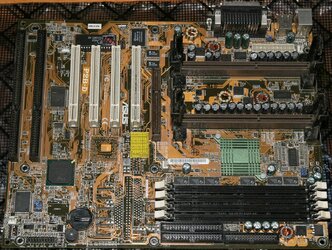
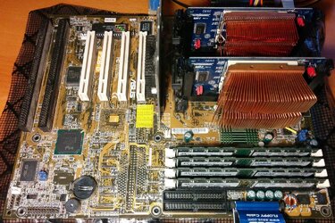
I will be using my 440BX based Asus P2B-D for this build which I bought over 16 years ago. It is revision 1.06 D03 which was the last hardware version made. The un-populated section is for the SCSI option available on the P2B-DS.
