• Welcome to Overclockers Forums! Join us to reply in threads, receive reduced ads, and to customize your site experience!

Q about SS and SOI

Overclockers is supported by our readers. When you click a link to make a purchase, we may earn a commission. Learn More.

Foxie3a

Normal Member
Joined
Sep 7, 2003
I've been reading a lot about SS and SOI but something is confusing me here.

I read how each one allows for higher clock speeds by upto **%. But does it allow you to go smaller. What I'm saying is, are they moving smaller just because they can lower the voltage, and also put up the clock, or are they going smaller JUST because you have to in order to use SS or SOI?

I hope that wasn't too confusing. :)

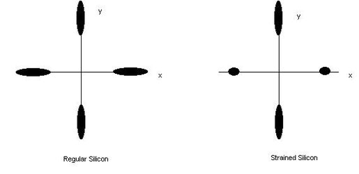
SS = Strained Silicon

SOI = Silicon On Insulator
 
The answer to your question simply is that SOI and SS are implemented strictly for speed. I would get more detailed but this stuff gets pretty deep. You would need some basic understanding of CMOS device physics to understand why SOI is used and device physics and some understanding of solid state physics/quantum mechanics to understand how SS works.

I could give you a more detailed explanation if you would like, but it would be a pretty big post even to get the basics of it.

As to why industry is continuing to move smaller is because smaller allows more packing density of the transistor, thus the chip can do more. Smaller transistors also mean less power, but with the increase in the number of components with each new technology node, the power this is kind of negated. Prescott is a good example, the number of transistors in the 1MB cache generates so much heat that it kind of negates to lower power consumption due to the move to a 90nm node, but then again parasitic effects at smaller devices can also lead to more heat, but this can often be corrected by improving on the fabrication process.
 
I got all that...I understand. So shoot away with your in depth explanation please. :)
 
Silicon on Insulator (SOI) has been used in silicon chips since 130 nm. Strained Silicon is not yet used in current chips (130 nm), will be used in future generations.

The following links give some basic introduction to the subjects.


Silicon on Insulator

hitechjb1 said:
Silicon-on-insulator (SOI)

SOI paper - A simple and clearly written article about silicon chips, traditional silicon process (bulk) and SOI, and the advantages of SOI on speed, power and soft error rate.

In addition, the article can serve also as an introduction to MOS, CMOS transistors, capacitance, scaling, ... in silicon chips, including nice illustrations and a cross-section of transistors in a SOI chip at down to 0.01-0.1 micron resolution.


Quote from the article:
"SOI technology improves performance over bulk CMOS technology by 25-35%, equivalent to two years of bulk CMOS advances. SOI technology also brings power use advantages of 1.7-3 times. IBM is currently working with many circuit designers and product groups that are designing with SOI technology. The company expects SOI will eventually replace bulk CMOS as the most commonly used substrate for advanced CMOS in mainstream microprocessors and other emerging wireless electronic devices requiring low power."


Strained Silicon

Quote from article: "A transistor built with strained silicon. The silicon is "stretched out" because of the natural tendency for atoms inside compounds to align with one another. When silicon is deposited on top of a substrate with atoms spaced farther apart, the atoms in silicon stretch to line up with the atoms beneath, stretching -- or "straining" -- the silicon. In the strained silicon, electrons experience less resistance and flow up to 70 percent faster, which can lead to chips that are up to 35 percent faster -- without having to shrink the size of transistors."

Strained Silicon article from IBM
Strained Silicon article from Intel
 
Last edited:
I know what the quotes say, but what you are saying is wrong. SS IS used in current chips. Ever hear of the P4 Prescott? Along with the chips IBM has made recently. The 790FX and the G-5's all use SS. So what you were saying is not true.

And yes, SOI is being used a lot now even.
 
Well this is going to take a while, will have to research some stuff just to make sure I get the facts right, but I will begin with an explanation of strained silicon since I am a little more familiar with this than SOI.

I will start off in this post with the concept of carrier mobility. Inside a semiconductor there are charged particles that dictate the electrical properties of the material. These particles are known as carriers and are introduced to the semiconductor though a process called doping. Doping is adding impurity atoms to a semiconductor that in turn place carriers in the semiconductor. There are two types of carriers, electrons that carry a negative charge and are the majority carrier in NMOS devices and holes that carry a positive charge and are the majority carriers in PMOS devices.

Carrier mobility is, effectively, the speed at which there carriers can move through the semiconductor lattice and is effected by the impurity/dopant concentration, electric field, and crystal orientation. High impurity concentrations lower the carrier mobility because there are more carriers present and their effective forward velocity is decreased due to greater chance of collision. Electric field limits the maximum mobility a carrier can have, thus if you have a high enough electic field your carrier mobility can saturate. Of imporatance to the discussion of strained silicon and why it can make a chip faster is crystal orientation. Most CMOS devices are created on a (100) crystal orientation due to lower atomic density when looking at the semiconductor from this orientation. This is imporant for the gate oxide used in the MOS capacitor that is the heart of a CMOS transistor. Lower atomic density means less chance of defects at the semiconductor/oxide interface. The problem lies in how carriers occupy their "permited" energy levels in a (100) oriented silicon lattice.

Well at this point I feel like I am doing homework :) so I will stop for now and let you digest the info i just gave. In my next post I will continue on how crystal orientation plays a role in carrier mobility and how strained silicon can increase carrier mobility thus the speed of the chip. Two terms you might want to look up between now and my next post is "effective mass" and "mass anisotropy." If you know what those mean it would make my job in explaining how strained silicon works a whole lot easier :D.
 
Read it all and am ready. Looking up the words now. :)
 
Good post Enigma422 - this is very interesting stuff.

Since you know a little about SS, I have a question. SS improves the mobility of electrons and allows for greater current density at an electric field relative to non-SS chips. Could this greater mobility, along with a decreased oxide layer at the 90nm feature size account for the increases in leakage current relative to the 130nm process?

What is your field of study anyways?
 
Foxie3a said:
Ok, found a good site for "Effective Mass"
http://en.wikipedia.org/wiki/Effective_mass

But I am having trouble with the other one, help?

Foxie3a, Effective mass is essentially what it says. Without going into complicated quantum mechanical equation, which I myself do not yet fully understand, effective mass is the mass that a particle exhibits with a given force applied to it. If we look at Newton's equation of force, for simplicity (this should not be used for the quantum regime, but I am using it as kind of a way to explain what happens.) F=ma and m=F/a. In free space, meaning that an electron or hole is no longer bonded to a crystal or atomic structure and can freely move where ever it wants, the energy space the electron occupies is circular in shape. This means that any force applied to the electron will result in the same mass in all directions. In a crystal plane however the shape becomes parabolic and thus if force is applied, the resulting acceleration in one direction, say the x direction, will not be the same as in the y direction. This is because a parabolic shape of the occupied space. The effective mass is the average mass computed from the acceleration of the particle with a constant force in all directions.

A picture of this would be helpful and I was going to post one, but apparently The Forum Is Down is no longer allowing uploads. I haven't been in this forum in a while so I don't know how long ago this happened. If anybody knows a link where I can upload pictures please let me know.

rudnik68 said:
Good post Enigma422 - this is very interesting stuff.

Since you know a little about SS, I have a question. SS improves the mobility of electrons and allows for greater current density at an electric field relative to non-SS chips. Could this greater mobility, along with a decreased oxide layer at the 90nm feature size account for the increases in leakage current relative to the 130nm process?

rudnik68, the leakage current with smaller dielectrics come mainly from parasitic effects that are harder to control as device sizes are scaled ever smaller. One main cause for leakage current, in terms of the MOS stack is that with a decreased oxide thickness there is a greater tendency for carriers to "tunnel" through the gate oxide from the gate electrode into the silicon. This is because at the scale that we are building transistors now the carriers become quantized and no longer follow the rules of classical physics. As you may or may not know, at the quantum level particles exhibit both particle and wave properties. It is the wave characteristics of the particles at this level that causes tunneling since with the extremely thin gate oxide used in todays 90nm process the wave function of the carriers in the gate electrode can overlap the gate oxide and fall into the semiconductor itself allowing carriers to essentially disappear from the gate electrode side of the capacitor and simultaneously appear in the semiconductor. This is why industry wants to move to high-k dielectrics for the gate because it allows for the high capacitance necessary to invert the charged carriers below the gate while allowing thicker dielectrics to prevent tunneling. Capacitance has an inverse relationship to oxide thickness so thinner oxide means more capacitance. the permiativity (sp) and capacitor area is directly related to capacitance, so a higher k value will allow for more capacitance with a thicker dielectric.

At the 90nm node there is less area thus more capacitance is needed than at the 130nm node. Thus the need for thinner gate oxides or high-k material as the CMOS is scaled down.

I will post more tonight, just wanted to get your new questions out of the way.


rudnik68 said:
What is your field of study anyways?

Well you must be wondering why I know this stuff :), well I am a couple months away from graduating with a degree in microelectronic engineering, and actually this kind of helps me remeber some of the stuff I have to know for one of the senior classes I am taking ;)
 
Last edited:
Enigma422 said:

Well you must be wondering why I know this stuff :), well I am a couple months away from graduating with a degree in microelectronic engineering, and actually this kind of helps me remeber some of the stuff I have to know for one of the senior classes I am taking ;)

What school do you go to? And is microelectronic engineering a undergrad or grad level course? I wish my university had a program in microelectronic engineering - probably woul have majored in that instead of chemical engineering.
 
Something like that may also be offered as a area of concentration under another major such as electrical or computer engineering. I myself am a CompE with concentrations in computer systems and VLSI (very large scale integration).
 
Well to continue where I left off......silicon wafers oriented in the (100) direction is what is used when fabricating CMOS transistors. Unfortunately for carriers this particular crystal orientation has a negative effect on mobility in the general direction that the carriers are moving. For my example I will be using electrons as the carrier.

In a silicon lattice electrons can occupy six distinct locations, two along the x direction, two along the y direction, and two along the z direction. From an energy vs. wave function (k) diagram of the silicon lattice in the (100) crystal orientation the shape of the locations the electrons occupy is parabolic in shape. The shape of the parabola with respect to the direction that the electron moves will effect the mobility of the electron. If the electron has to travel along the longer part of the parabola in a given electric field the mobility of the electron will go down. On the other hand if the distance traveled is along the shorter part of the parabola the mobility will go up. I attached a file that will shows how electons occupy the silicon lattice in two dimensions. If the applied electric field travels along the x direction the concept you can see that the electrons occupying the states in along the x-axis has to travel a longer distance than the electrons that occupy the states on the y-axis. This is because the shape of the state is more parabolic along the x-axis and more circular along the y-axis with the electric field running in the x-direction. This phenomenom is known as mass anisotropy. This is because the effective mass of the electrons that occupy the states on the y-axis will have a different effective mass than the electrons that occupy the states along the x-axis. The overall effective mass is the average of the x-axis effective mass, the y-axis effective mass, and the z-axis effective mass (not shown). Its a little more complicated than I made it out to be, but as long as you can see the concept. This is basically what a lot of my college career is based upon so it would kind of be hard to fit everything in one post.

Now that you understand how electrons travel slower based on the state that they occupy and the direction that they are traveling I can explain what strained silicon does. Essentially what strained silicon does is change the shape of the parabola, especially the ones that occupy the states along the x-axis (with respect to my diagram) This is because when you add have a silicon germanium semiconductor you not only change the lattice constant, essentially stretching the lattice, but you also change the energy vs. wave function diagram of the semiconductor resulting in less parabolic shaped along the x-axis. Since the electrons now have less of a distance to travel their mobility goes up, thus increasing the current drive in the transistor. In my attached file the standard case is on the left and the strained case is on the right.

Hope that this was adaquate explaination. I myself am still learning about this stuff and it took a lot of background courses to be able to understand the concepts, and obviously I can't fit all of the information in a post (it's a lot of stuff :)). Anyway this should at least give you an idea on why Intel has moved to strained silicon and how it effects transistor performance on the semiconductor level.

Any questions feel free to ask and I will try to answer them to the best of my ability. Any corrections feel free to tell me. Just don't expect me to teach you everything about semicondutor physics. That's what you go to college for ;).

Intel has a nice presentation that includes better diagrams of my explanation. Scroll down to 8th slide and a three dimensional diagram of my attachment is shown as well as a basic explanation.

Next time, I will tackle SOI. This should be an easier explanation than strained silicon.
 

Attachments

  • strained silicon.jpg
    strained silicon.jpg
    6.8 KB · Views: 85
rudnik68 said:


What school do you go to? And is microelectronic engineering a undergrad or grad level course? I wish my university had a program in microelectronic engineering - probably woul have majored in that instead of chemical engineering.

Hey rudnik68, I go to RIT, and it's an undergrad program. I think my major is the only undergrad microelectronic engineering program in the US. I believe Stanford has one, but I am not sure if it is undergrad and grad or just grad. I do know that it was the first and it is the best. We also have the most complete fabrication laboratory of any other university. The best part is that you can use it as an undergrad, unlike other univerisities that restrict the use of such a lab to the graduate program.

You would be surprise how much of a chemisty is involved in semiconductor fabrication is. :D
 
Last edited:
Enigma422 said:
In a silicon lattice electrons can occupy six distinct locations, two along the x direction, two along the y direction, and two along the z direction. From an energy vs. wave function (k) diagram of the silicon lattice in the (100) crystal orientation the shape of the locations the electrons occupy is parabolic in shape. The shape of the parabola with respect to the direction that the electron moves will effect the mobility of the electron. If the electron has to travel along the longer part of the parabola in a given electric field the mobility of the electron will go down. On the other hand if the distance traveled is along the shorter part of the parabola the mobility will go up. I attached a file that will shows how electons occupy the silicon lattice in two dimensions. If the applied electric field travels along the x direction the concept you can see that the electrons occupying the states in along the x-axis has to travel a longer distance than the electrons that occupy the states on the y-axis. This is because the shape of the state is more parabolic along the x-axis and more circular along the y-axis with the electric field running in the x-direction. This phenomenom is known as mass anisotropy. This is because the effective mass of the electrons that occupy the states on the y-axis will have a different effective mass than the electrons that occupy the states along the x-axis. The overall effective mass is the average of the x-axis effective mass, the y-axis effective mass, and the z-axis effective mass (not shown). Its a little more complicated than I made it out to be, but as long as you can see the concept. This is basically what a lot of my college career is based upon so it would kind of be hard to fit everything in one post.
This is the only part of your post I don't understand. Are these 6 locations the electrons can ocupy the orbitals? It sounds like it, but I've been out of chem too long to remember just how many Silicon has, and what shape they're in :D The hardest part is visualizing exactly what's going on when the electrons move, which is obviously the hardest part to convey in a written medium....


Enigma422 said:
You would be surprise how much of a chemisty is involved in semiconductor fabrication is. :D
Not really, I'd think chemistry would be essential in getting everything correct. Especially with sub-micron (gate?) sizes....

JigPu
 
Sorry I haven't updated this post for those of you who are intereted. Been a busy week for me, but I hopefully will be able to post something on SOI this weekend.

JigPu said:

This is the only part of your post I don't understand. Are these 6 locations the electrons can ocupy the orbitals? It sounds like it, but I've been out of chem too long to remember just how many Silicon has, and what shape they're in :D The hardest part is visualizing exactly what's going on when the electrons move, which is obviously the hardest part to convey in a written medium....


Not really, I'd think chemistry would be essential in getting everything correct. Especially with sub-micron (gate?) sizes....

JigPu

Effective mass is a concept I am trying to learn myself, it is part of a course I am taking on deep submicron CMOS technology. Will see what I can find in my notes and text and get back with hopefully a better explaination, but from what I understand they are not orbitals, but are allowed energy states an electron can occupy in a silicon lattice. It comes from an three dimensional representation of the energy vs. wave number (E-k diagrams). Not sure if they relate to orbitals or not, but I will try to look that up.
 
Back