• Welcome to Overclockers Forums! Join us to reply in threads, receive reduced ads, and to customize your site experience!

Come get your 4870 Review's =D

Overclockers is supported by our readers. When you click a link to make a purchase, we may earn a commission. Learn More.
Actually the GDDR5 that ATI is using is quad data rate so QDR. Its shown on the card as 900Mhz stock clock, yet its effective DDR3 speed is 3.6Ghz so overall if you want to be get dirty and "match" it to ddr3 thats where the 2.3Ghz comes from or the 900Mhz which ever you want to consider.

Where does it show 900MHz on the card?

And how is QDR even possible if DDR uses the rising and falling edge of the clock. There's no more edges to work with. :confused:
 
Where does it show 900MHz on the card?

And how is QDR even possible if DDR uses the rising and falling edge of the clock. There's no more edges to work with. :confused:

Guess I don't know how to explain that one. All I know is what I was reading on it. There can be 3 speeds you can get actual numbers on the card.

Since surely someone can show it, when you OC it from the tool bar or something it should be reading 900Mhz default on the 4870.


Edit:
Ah here is one showing an OC result on the 4870.
http://firingsquad.com/hardware/ati_radeon_4850_4870_performance/page16.asp
As you see for the 4870 its listed at 1100Mhz, so really its 2200 or 4400Mhz DDR speed dependin which way you want to take it.

Think its similar to what Rombus is trying to pull out with theres. While they plan on hitting like 1Thz+ with there new chips but the chip itself is only running 333-500Mhz itself. There taking into account that the new chips process more information in a cycle.
 
Last edited:
All the reviews I have seen have called it 900mhz memory with an effective speed of 3600mhz. They don't really explain why though..
 
All the reviews I have seen have called it 900mhz memory with an effective speed of 3600mhz. They don't really explain why though..
It must be a 1:2 multiplier which affects the real clock, which then yields the effective clock.

I KNOW another video card has a multiplier(software or hardware, who knows, hopefully software) like this years ago... but I don't remember who made it or what it was... I don't think it was ATi or nVidia... that's going to bother me until I forget about it.
 
Where does it show 900MHz on the card?

And how is QDR even possible if DDR uses the rising and falling edge of the clock. There's no more edges to work with. :confused:


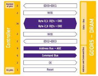
It actually has 2 separate write clocks using the rising and falling edge of the clock. Which means more wires to the memory controller if I'm not mistaken. Plus they tweak other things so it clocks better like another clock just for addressing and commands.

wikipedia said:
2617340348_b63d5654eb_o_d.jpg

GDDR5 (Graphics Double Data Rate, version 5) is a type of graphics card memory. It will be the successor to GDDR4. Unlike its predecessors, GDDR5 has two parallel DQ links that provide doubled I/O throughput compared to GDDR3 and GDDR4.

Here is a link to the qimonda white paper http://www.qimonda-news.com/download/Qimonda_GDDR5_whitepaper.pdf
 
Ugh, I'd typed out a reply with references but it didn't post for some reason. Yes it is effectively QDR from the base 'SDR' clock speed, how it gets there isn't important. DDR sends signals on the rising and falling edge and GDDR5 sends twice the info per signal of DDR, at least that's how I understand it. That's why some sites are starting to quote MT/s = megatransfers/second instead of MHz, it's an easier way to compare across technologies.

Here's a better wiki link: http://en.wikipedia.org/wiki/GDDR5
 
Last edited:
Ugh, I'd typed out a reply with references but it didn't post for some reason. Yes it is effectively QDR from the base 'SDR' clock speed, how it gets there isn't important. DDR sends signlas on the rising and falling edge and GDDR5 sends twice the info per signal of DDR, at least that's how I understand it. That's why some sites are starting to quote MT/s = megatransfers/second instead of MHz, it's an easier way to compare across technologies.

Here's a better wiki link: http://en.wikipedia.org/wiki/GDDR5

Beat you to it :santa:
 
Thanks for the explanation fellas!

Very informative. Makes a lot more sense now, b/c it seemed bewildering to me how they could get the speed up that fast in such a short period of time. They basically increased the bus width w/n the RAM, so if you think about it the 4870 kind of has a 512-bit bus since it's a 256-bit bus w/ twice the lanes to the memory.

Yea it's pretty slick and obviously a lot more of an increase than GDDR4. I wonder if NV has a GDDR5 controller laying nascent in the GT200 or if it can be added on or is somehow compatible with GDDR3...it may be given the AMD seems to have no problem using GDDR3 on the 4850 and GDDR5 on the 4870 or they've included both controllers. If NV didn't include that and they stick with the GT200 as a basis for a year they will have problems.
 
Back