• Welcome to Overclockers Forums! Join us to reply in threads, receive reduced ads, and to customize your site experience!

My toasted L5 bridge and request for pics of correctly burned bridges on newer barton

Overclockers is supported by our readers. When you click a link to make a purchase, we may earn a commission. Learn More.

314

Registered
Joined
Feb 17, 2004
My toasted L5 bridge and request for pics of correctly burned bridges on newer barton

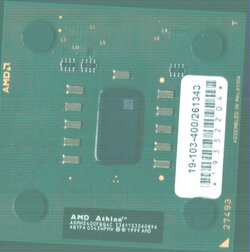
Call me a guinea pig. I took the bait and ordered some new athlon mobiles to put in a duallie K7D Master. Little did I know that there seem to be no pics anywhere on the web of correctly burned bridges for these post week 39 2003 Bartons. SOMEBODY WRITE A DETAILED GUIDE / STICK ALREADY!

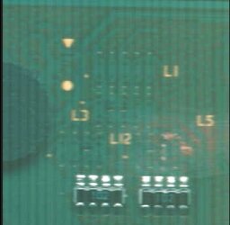
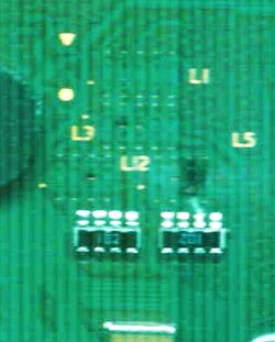
Anyway, in my particular case I needed to burn the 3rd L5 bridge to undo the PowerNow! feature. There are four dots per bridge: two on the outside and two on the inside. All of them are under a coating of enamal or plastic. At first I tried applying 6 volts to the outer pins. According to my K7D they still were not recognized as MPs. So then I tried applying 6 v to the inner pins of the 3rd bridge. Here the needles got red hot.:eek: I switched to a thicker conductor and eventually managed to burn a big chunk of copper out of the approximate place were I think the bridge was. In truth I was arc welding at this point.:mad: But no luck with the chip being recognized as an MP. Attached is what resulted after many hours.

It is sort of tough to see, but basically there is a DEEP hole where I think I was supposed to cut.

So are the inner or outer pins the ones to use? SMP Q: What is the easiest way to know once this mod has been correctly done? Also, can somebody tell me how to do this with a knife? And how about what is down below in this area of the chip? Can I stop digging when I can see the other side?:p Anyone with a successfull mod please post a pic.
J
 

Attachments

  • psd_70c3.jpg
    psd_70c3.jpg
    57.3 KB · Views: 300
"I needed to burn the 3rd L5 bridge to undo the PowerNow! feature" - I do not understand why you wanted to disable PowerNow!. AMD761 chipset supports PowerNow! and AMD762 should also support it (one man told me this). That way you would be able to change multiplier from operating system on each of the processors individually. There is no reason why to disable this feature unless your motherboard's BIOS is so stupid it refuses to work with mobile CPUs.
 
Petr: The MP/MPX chipsets do not properly support PowerNOW!

In uniprocessor mode, it sets the multipler and vcore both to maximum, and you cannot decrease them. You can hit "apply" to set a new multiplier but it won't stick. In SMP mode, it just won't POST. Noone has managed to get two mobile CPUs to POST in a SMP board.

Hence you need to break the 3rd L3.

There are many tutorials out there about joining bridges when you have the laminated packaging (though this came in before the locked chips). Typically, you need to CAREFULLY scrape the laminate off the inner two dots (the outer two are just joined to ground), fill in the gap with an insulator, then rejoin as per normal. To cut the bridges, you just need to scrape the bridge *in the direction of the bridge* until it registers as broken with a multimeter. You can do it across the bridge, but you need a lot more skills and balls as it's very easy to slip and slice the wrong wire.

The bridges are quite thin, so not much scraping is needed. And if you go too deep, you can hit the ground plane and pull the bridge permanently to ground, which is not a good thing. However, from various Athlon destruction photos, I don't think there's anything directly beneath the bridges. I still wouldn't recommend going through to the back, though :)

In this case, I suspect that the OP has damaged the bridge sufficiently to pull it to ground. with all the smoked material in there. This is why zapping it with electricity is a bad idea, and IMO should never be used. To fix it will require cutting the bridge using a needle (or similar object with a sharp tip) "further up" the line (towards the outside of the chip in the case of the L5's, IIRC). I haven't looked at a closeup of the bridge areas in a while, so possibly you need to cut the other side. If the OP could post a closeup of the bridges, it'd be easier to assess the damage and suggest a good place to cut.
 
warlock110 said:
ahhh damm, that's a huge hole u made, is the chip still working?

Good question. Strangly, yes. No difference that I can tell. Then again, realize the CPU wasn't touched.

J
 
Do both CPUs actually post and work? The fact that they aren't recognized by the BIOS is insignificant as long as you can actually run both chips in the mobo
 
Petr said:
"I needed to burn the 3rd L5 bridge to undo the PowerNow! feature" - I do not understand why you wanted to disable PowerNow!. AMD761 chipset supports PowerNow! and AMD762 should also support it (one man told me this). That way you would be able to change multiplier from operating system on each of the processors individually. There is no reason why to disable this feature unless your motherboard's BIOS is so stupid it refuses to work with mobile CPUs.

i did? lol or do u mean another person? but ya that hole is pretty big :(
like coolest said as long as they can run stable its all good the name isnt that huge off a deal, wow coolest 2.1ghz? at 1.9v wow thats crazy
must have been a bad proc eh?
 
emboss said:
Hence you need to break the 3rd L3.

I think you meant the 3rd L5 here? I toasted the 3rd bridge above the 11 o'clock 201. The newer labelling on these chips isn't clear.

There are many tutorials out there about joining bridges when you have the laminated packaging (though this came in before

If you know of any links with pics and or resistance bridge readings on these laminated chips that would be nice to see.

Thanks a mil for answering the innie outtie q. That helps a great deal. Seems I blew the outer bridge as well.

using a needle (or similar object with a sharp tip) "further up" the line (towards the outside of the chip in the case of the L5's, IIRC). I haven't looked at a closeup of the bridge areas in a while, so possibly you need to cut the other side. If the OP could post a closeup of the bridges, it'd be easier to assess the damage and suggest a good place to cut.
Attached is the highest resolution my scanner can do of the other chip. Hope somebody else posts a pic or 2.
 

Attachments

  • l5chip2.jpg
    l5chip2.jpg
    20.7 KB · Views: 242
And here is the original chip at highest res.
 

Attachments

  • l5chip1.jpg
    l5chip1.jpg
    32.7 KB · Views: 236
wquiles said:
These are pictures of my recently received Mobiles and also comparison pictures of my older (current) Tbreds. Does this helps some?

I will be attempting the modification to enable SMP today or tomorrow.

http://www.ocforums.com/showthread.php?s=&threadid=279294

So basically, the proper technique is to short the "inner" dots after I have scraped them, right?

After my arc welding yesterday and blistered hands from burn marks I would have to say don't use current but use a needle to scratch. I am guessing here however since I haven't been able to get it to work and am waiting for someone to post of link or picture of how to best do this.

J
 
I repeat: do NOT use electricity to blow the bridges. Scrape (lightly) along the direction of the bridges with a needle. Try not to dig the needle into the chip (ie: if you meet resistance, don't push harder) otherwise you'll start digging up the ground plane too, and this could cause problems. If you do it carefully, you should see a change in colour as you start scraping the substrate. Stop once there is a constant line of "substrate" colour across the bridge. I strongly recommend you do this under a low-power microscope or decent magnifying glass.

When I was cutting bridges as part of the post week-39 unlocking effort, I used a microscope on 100x power, a sharp needle, and a 100w lamp for illumination and heating. The laminate comes off easier when it's warmer, but don't get it hot enough to damage the chip. It took some patience and time, but it's not too difficult with the right equipment.
 
Why on earth would someone want to use electricity to blow up bridges on a sensitive component like a CPU? I'll never understand that. A x-acto knife (or razor blade) and a magnifier are all you need.
 
stamasd said:
Why on earth would someone want to use electricity to blow up bridges on a sensitive component like a CPU? I'll never understand that. A x-acto knife (or razor blade) and a magnifier are all you need.

Because there aren't enough people like you! Serously, you experienced guys haven't been telling us SMPers any better, so we just were following Chris's duallie guide (which was until today very pro-electric) and Rav (see here). One of the reasons for me posting on the non-SMP side of things was to try to get some outside opinions. Now it seems clear that anyone applying current to a new chip is either an idiot or into basic research on chip design.

Situation is not unlike the Chinese emperor who walked around naked.

PLEASE TELL ME HOW TO DO THIS USING A KNIFE AND UPLOAD A PIC OF A PROPERLY CUT BRIDGE.

J
 
I've already explained twice how to do it. It's not that hard.

I can't upload a photo for two reasons:
(1) I don't want to disassemble and reassemble my entire case to remove one of my CPUs. Last time I did it the entire process took about 6 hours: I've done a fair bit of ducting and removing the CPU requires just about COMPLETE disassembly of my case.
(2) Even if I did have the time, I don't have access to a good enough scanner to take a decent picture. To accurately see what I've done would require an optical resolution of ~4000dpi (otherwise you just end up with the blurry mush like your scans). Scanners of this quality are ~$1000 here in NZ, so very few people have them.

A 10-second search of google also turned up
http://www.overclockers.com/tips1107/
which explains another way of doing it, with a couple of diagrams. I personally wouldn't try soldering your chip, as using conductive paint is a far safer way of doing it.
 
emboss said:
I've already explained twice how to do it. It's not that hard.
...
A 10-second search of google also turned up
http://www.overclockers.com/tips1107/
which explains another way of doing it, with a couple of diagrams. I personally wouldn't try soldering your chip, as using conductive paint is a far safer way of doing it.

Thanks, that link is just what I was looking for. It helps a great deal. Since I need to open a bridge, I agree that isn't what I need to do. But it at least tells me the basics of what is going on.

Jason
 
Back