- Joined
- Feb 18, 2010
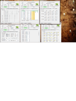
So I am wanting to increase voltage on my card (EVGA gtx 770). I would like to keep the voltage scaling with clock speed feature and not a 24/7 static voltage. I am assuming that the voltage table corresponds with the boost table seeing as the number of entries match. There are 7 other voltage adjustments on the voltage table that have no designation, what are these for?
There are 9 sections (3 entries each min,def,max) in the power table. They are not in any apparent order. I have seen a few posts that suggest certain ones are for rail power targets, and one for the core, and so on, but they seemed to have less entries on their bios so I am not certain. Any clarification on this would be appreciated.
Now on the common tab there are entries for TDP Base Entry, 3D Base Entry, and Boost Entry, as well as TDP base clock. They are directed to entry 1, entry 1, and entry 0 respectively. Is this where the change to TDP of the card is made by adjusting their corresponding entry, or does this not even matter and the power table section is where the changes are made? Also I am assuming that the entry selection references the clock state section.
I have provided a screenshot to aid in assistance. Any help or guidance would be greatly appreciated.