• Welcome to Overclockers Forums! Join us to reply in threads, receive reduced ads, and to customize your site experience!

Anybody see new Rev E specific dividers?

Overclockers is supported by our readers. When you click a link to make a purchase, we may earn a commission. Learn More.
Super Nade said:
Do the reserved values have to take numbers < 200MHz or can they be anything? If they can be anything, the answer could be, CPUz etc are confused by utilization of these reserved values.

These reserved values have known ratios (they're the "183MHz", "150MHz", etc etc values). They are all known and detected by CPU-Z and the like. I don't know if anyone has done exhaustive tests using A64Tweaker or similar to verify that the rev E's have the same speeds in the reserved slots, but so far it appears that AMD has added an extra bit somewhere. CPU-Z etc don't know about this extra bit (and AMD neither document it nor responded to my questions about it) so the easiest way to find out would be by someone with a DFI and a rev E doing MSR dumps at various RAM settings. PM me if you want the program to do this (Win32 or boot CD/floppy only).{EDIT}Sorry, misremembered. Boot floppy (or Win9x DOS mode) only. Also, the memory controller is set up through the PCI configuration registers, not the MSRs, so probably more useful would be a wpcredit dump of bus 0 device 24 functions 2 and 3.{/EDIT}

There could be a couple reasons for the low performance. Although I was fairly confident the crossbar operated at the core frequency, there is a possibility that it operates at the system or hypertransport frequencies. This could bottleneck the RAM to 6400MBytes/sec and thus would prevent the higher-than-1:1 ratios from giving much more bandwidth. Alternatively, the CPU<->XBAR or memory<->XBAR pipes could be limited for various reasons, causing similar issues.
 
Last edited:
emboss said:
These reserved values have known ratios (they're the "183MHz", "150MHz", etc etc values). They are all known and detected by CPU-Z and the like. I don't know if anyone has done exhaustive tests using A64Tweaker or similar to verify that the rev E's have the same speeds in the reserved slots, but so far it appears that AMD has added an extra bit somewhere. CPU-Z etc don't know about this extra bit (and AMD neither document it nor responded to my questions about it) so the easiest way to find out would be by someone with a DFI and a rev E doing MSR dumps at various RAM settings. PM me if you want the program to do this (Win32 or boot CD/floppy only).

There could be a couple reasons for the low performance. Although I was fairly confident the crossbar operated at the core frequency, there is a possibility that it operates at the system or hypertransport frequencies. This could bottleneck the RAM to 6400MBytes/sec and thus would prevent the higher-than-1:1 ratios from giving much more bandwidth. Alternatively, the CPU<->XBAR or memory<->XBAR pipes could be limited for various reasons, causing similar issues.

:thup:

I was about to post the exact same question but you have done an excellent job (as always), of putting it in a coherent fashion.

Additionally,I was under the impression that the crossbar switch always operated at a multiple of 200MHz? So, if what you say is correct, this bottleneck can be quantified by raising the LDT, right? I mean, higher hypertransport freq should net higher points?

Could you explain what the orange text in my earlier post means? Why would AMD say that these bits can take up higher values?
 
Last edited:
After a bit more thought, I'd say that the crossbar does not operate at the hypertransport frequency. Why? There have been several articles where people have investigated the effect of changing the hypertransport multipliers. See
http://www.neoseeker.com/Articles/Hardware/Guides/athlon64oc/2.html
for example. None of these show any significant change in Sandra memory benchmarks, going from 1x to 5x. This is not what would be expected if the RAM bandwidth was being cut by a factor of 5. This doesn't rule out the possibility of it running at a constant multiple of the system clock, which would cause it to have a restricted bandwidth on each port.

There's two experiments that could shed light on this. The first would require an dual-Opteron system and a bit of research to see how XP NUMA support works. Essentially, it'd be a RAM bandwidth test that would run on a single CPU, but hit RAM from both CPUs. If the CPU port was restricted to 6.4GBytes/sec, this would be obvious in the bandwidth readings, which should be around 10GBytes/sec (~5 from local ram and ~5 from the remote RAM over hypertransport).

The second test could run on an X2 or a dual-Opteron. This would work by having two threads, one for CPU0 and one for CPU1. The first thread would generate, say, 512KB of data. Obviously, this would reside in the cache of CPU0. Once the first thread had generated the data, the second thread would start, and read in both the data from the first thread (hence requiring it to be transferred over the hypertransport bus) and also data from main memory. Again, this would show up as a reduced overall bandwidth if the CPU or crossbar bandwidth is constrained.

A variant of this test could be interesting as well. Essentially the same, except CPU1 just reads the data from CPU0. Essentially testing the bandwidth between the two CPUs. If the crossbar operated at a frequency higher than the hypertransport link and the X2 operates as AMD claims (where the second CPU is directly bolted onto the crossbar, not going through a hypertransport link), the X2 whould have more CPU<->CPU bandwidth than the dual Opteron system.

Back to the topic, where does that leave us? Well, there's two options:
1) Memory controller <-> CPU bandwidth limited in some way.
2) Higher than 1:1 ratios are not implemented properly.

I personally find option 1 much more likely. Since all AMD have done is add an extra few columns to a divider table, there should be no difference in operation of the memory controller between 200 and 250Mhz settings. All that is different is the divider. But if option 1 is the case, AMD has done some very strange things. For example, what would be the point of the 5x hypertransport multiplier, and the higher than 1:1 memory ratios? Clearly, something is bottlenecking below 6.4GBytes/sec, which would suggest a crossbar multiplier and bus width that would limit to 256 bits per system clock cycle (eg: 8x at 32 bits wide, 4x at 64 bits wide, etc).

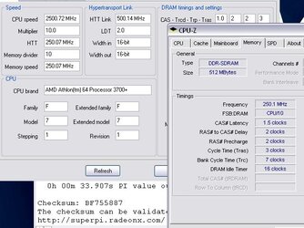
Back to the orage text, this is referring to the early Opterons. These chips had a memory bus limit of 166MHz (PC2700), and reported this as such in the DramFreq field. All that the orage text is saying is that DramFreq is indicitive, not restrictive. You can tell these early Opterons to use a 200MHz RAM frequency, even if they tell you that they can't go above 166MHz. Thay just probably won't work correctly :)
 
Super Nade said:
I'm not going to be using any 7-x BIOS! I think deception's CPU was killed by the VCore bug.

hitech, I saw your updated post. I was just wondering if any BIOS supports it and if so what are the consequences in the relam of stability,VCore required etc..

Sorry, I guess I should have updated that thread.....

It turns out my processor was not killed due to the 7/04 bios. Oddly enough, it was my OCZ PC 4800 that bit the bullet. I tried some of my old Mushkin Bh-5 in the same system and everything went back to normal. Currently, I have not been very active, as my OCZ is on its way back to me from RMA.

deception``
 
Super Nade

What would a SuperPi time test (say 1M) yeild?

Here we go :)

200X1011.JPG = 200 HTT X 10 CPUX, 200 MHz / 1:1 "ratio" - 41.985s
200X1076.JPG = 200 HTT X 10 CPUX, 233 MHz / 7:6 "ratio" - 41.672s
200X1054.JPG = 200 HTT X 10 CPUX, 250 MHz / 5:4 "ratio" - 41.141s
233X1011.JPG = 233 HTT X 10 CPUX, 200 MHz / 1:1 "ratio" - 36.313s
250X1011.JPG = 250 HTT X 10 CPUX, 200 MHz / 1:1 "ratio" - 33.907s

These ratios definitely increase performance above our reference memory speed of 200 MHz. The 233x10 and 250x10 results are somewhat meaningless, for this specific comparison, because SuperPi is heavily affected by CPU frequency. I've stuck to the same multiplier, and the exact same settings as were used for the Sandra bandwidth benchmarks (2x256 Megs BH-5 @ 1.5-2-2-3, tight secondary timings, tREF 3120).

Now I want to know what these ratios actually set our memory frequency to, so I can start doing some stability testing near the upward-limits of my memory. I wonder, will a low HTT improve memory overclocking potential? :)

Also, I would really like to see all of these little tests repeated, but with an FX-57.
 

Attachments

  • 200X1011.JPG
    200X1011.JPG
    55.8 KB · Views: 394
  • 200X1076.JPG
    200X1076.JPG
    53.5 KB · Views: 380
  • 200X1054.JPG
    200X1054.JPG
    55.2 KB · Views: 377
  • 233X1011.JPG
    233X1011.JPG
    57 KB · Views: 376
  • 250X1011.JPG
    250X1011.JPG
    56.2 KB · Views: 377
Last edited:
A little program called A64-Info (I found this program through the thread on this topic, over on XS) gives us a little bit more information.

It also seems to be detecting incorrect memory frequencies, although it tells us more than CPU-Z or memtest86.

Get it here: http://www.digitalonline.co.yu/Spekta/A64Info.rar

A64-Info screens for 200x10, 233 MHz/7:6 and for 200x10, 250 MHz/5:4.
 

Attachments

  • A64Info200x1076.JPG
    A64Info200x1076.JPG
    52 KB · Views: 395
  • A64Info200x1054.JPG
    A64Info200x1054.JPG
    51.5 KB · Views: 392
OK, that's interesting. AMD appears to be reusing some of the bits:
216MHz = 000
233MHz = 001
250MHz = 010
Now we just gotta find out the bit they are using to select between the low and high ranges. Could you do a wpcredit dump (copy'n'paste) for the 233, etc multipliers please felinusz? :)
 
Here are the WPCredit values for the memory controller, across the three ratios :)


200 MHzx10, 200 MHz/1:1 Ratio

----------------------------------------------------------
WPCREDIT Version 1.4 / Copyright (c) 1998-2004 By H.Oda!
----------------------------------------------------------
PCI Bus : 0 Vendor ID: 1022
Device : 24 Device ID: 1102
Function: 2 Revision : 00 Host Bridge
----------------------------------------------------------
00 01 02 03 04 05 06 07 08 09 0A 0B 0C 0D 0E 0F
+ -- -- -- -- -- -- -- -- -- -- -- -- -- -- -- --
00 | 22 10 02 11 00 00 00 00 00 00 00 06 00 00 80 00
10 | 00 00 00 00 00 00 00 00 00 00 00 00 00 00 00 00
20 | 00 00 00 00 00 00 00 00 00 00 00 00 00 00 00 00
30 | 00 00 00 00 00 00 00 00 00 00 00 00 00 00 00 00
40 | 00 00 00 00 00 00 00 00 01 00 00 00 00 00 00 00
50 | 00 00 00 00 00 00 00 00 00 00 00 00 00 00 00 00
60 | 00 00 00 00 00 00 00 00 00 FE E0 01 00 00 00 00
70 | 00 00 00 00 00 00 00 00 00 00 00 00 00 00 00 00
80 | 40 00 00 00 00 00 00 00 00 24 32 02 10 03 00 00
90 | 22 CC 05 2E 07 C6 73 3E 00 00 37 61 00 00 00 00
A0 | 00 00 00 00 00 00 00 00 00 00 00 00 00 00 00 00
B0 | F3 A7 60 71 E0 00 00 00 CF 9F C2 00 30 3A 93 43
C0 | 00 00 00 00 00 00 00 00 00 00 00 00 00 00 00 00
D0 | 11 06 35 B2 19 90 2A 2D 09 BC 70 4E 0C 17 98 4A
E0 | 0C 82 B9 A3 03 6A E6 10 30 8A 7D 37 01 03 29 87
F0 | 00 00 00 00 00 00 00 00 00 00 00 00 00 00 00 00
----------------------------------------------------------

----------------------------------------------------------
WPCREDIT Version 1.4 / Copyright (c) 1998-2004 By H.Oda!
----------------------------------------------------------
PCI Bus : 0 Vendor ID: 1022
Device : 24 Device ID: 1103
Function: 3 Revision : 00 Host Bridge
----------------------------------------------------------
00 01 02 03 04 05 06 07 08 09 0A 0B 0C 0D 0E 0F
+ -- -- -- -- -- -- -- -- -- -- -- -- -- -- -- --
00 | 22 10 03 11 00 00 00 00 00 00 00 06 00 00 80 00
10 | 00 00 00 00 00 00 00 00 00 00 00 00 00 00 00 00
20 | 00 00 00 00 00 00 00 00 00 00 00 00 00 00 00 00
30 | 00 00 00 00 00 00 00 00 00 00 00 00 00 00 00 00
40 | FF 3B 00 00 40 00 00 00 00 00 00 00 00 00 00 00
50 | 88 5A 24 F1 00 00 00 00 00 00 00 00 C0 7F B4 FB
60 | FB 00 00 00 00 00 00 00 00 00 00 00 00 00 00 00
70 | 11 01 02 51 11 80 00 50 00 38 00 08 1B 22 00 00
80 | 00 00 07 23 13 21 13 21 00 00 00 00 00 00 00 00
90 | 00 00 00 00 41 08 00 00 80 11 80 74 00 00 00 00
A0 | 00 00 00 00 00 00 00 00 00 00 00 00 00 00 00 00
B0 | 00 00 00 00 00 00 00 00 3F 00 00 00 00 00 00 00
C0 | 00 00 00 00 00 00 00 00 00 00 00 00 00 00 00 00
D0 | 00 00 00 00 07 A7 FF 00 00 00 00 00 00 00 00 00
E0 | 00 00 00 00 20 06 54 0A 19 05 00 00 00 00 00 00
F0 | 00 00 00 00 00 00 00 00 00 00 00 00 00 00 00 00
----------------------------------------------------------

200 MHzx10, 233 MHz/7:6 Ratio

----------------------------------------------------------
WPCREDIT Version 1.4 / Copyright (c) 1998-2004 By H.Oda!
----------------------------------------------------------
PCI Bus : 0 Vendor ID: 1022
Device : 24 Device ID: 1102
Function: 2 Revision : 00 Host Bridge
----------------------------------------------------------
00 01 02 03 04 05 06 07 08 09 0A 0B 0C 0D 0E 0F
+ -- -- -- -- -- -- -- -- -- -- -- -- -- -- -- --
00 | 22 10 02 11 00 00 00 00 00 00 00 06 00 00 80 00
10 | 00 00 00 00 00 00 00 00 00 00 00 00 00 00 00 00
20 | 00 00 00 00 00 00 00 00 00 00 00 00 00 00 00 00
30 | 00 00 00 00 00 00 00 00 00 00 00 00 00 00 00 00
40 | 00 00 00 00 00 00 00 00 01 00 00 00 00 00 00 00
50 | 00 00 00 00 00 00 00 00 00 00 00 00 00 00 00 00
60 | 00 00 00 00 00 00 00 00 00 FE E0 01 00 00 00 00
70 | 00 00 00 00 00 00 00 00 00 00 00 00 00 00 00 00
80 | 40 00 00 00 00 00 00 00 00 24 32 02 10 03 00 00
90 | 22 CC 05 2E 07 C6 93 3E 00 00 37 61 00 00 00 00
A0 | 00 00 00 00 00 00 00 00 00 00 00 00 00 00 00 00
B0 | B4 24 B5 B8 1C 00 00 00 CF 9F C2 00 30 3A 93 43
C0 | 00 00 00 00 00 00 00 00 00 00 00 00 00 00 00 00
D0 | 11 06 35 B2 19 90 2A 2D 09 BC 70 4E 0C 17 98 4A
E0 | 0C 82 B9 A3 03 6A E6 10 30 8A 7D 37 01 03 29 87
F0 | 00 00 00 00 00 00 00 00 00 00 00 00 00 00 00 00
----------------------------------------------------------
----------------------------------------------------------
WPCREDIT Version 1.4 / Copyright (c) 1998-2004 By H.Oda!
----------------------------------------------------------
PCI Bus : 0 Vendor ID: 1022
Device : 24 Device ID: 1103
Function: 3 Revision : 00 Host Bridge
----------------------------------------------------------
00 01 02 03 04 05 06 07 08 09 0A 0B 0C 0D 0E 0F
+ -- -- -- -- -- -- -- -- -- -- -- -- -- -- -- --
00 | 22 10 03 11 00 00 00 00 00 00 00 06 00 00 80 00
10 | 00 00 00 00 00 00 00 00 00 00 00 00 00 00 00 00
20 | 00 00 00 00 00 00 00 00 00 00 00 00 00 00 00 00
30 | 00 00 00 00 00 00 00 00 00 00 00 00 00 00 00 00
40 | FF 3B 00 00 40 00 00 00 00 00 00 00 00 00 00 00
50 | 88 5A 24 F1 00 00 00 00 00 00 00 00 C0 7F B4 FB
60 | FB 00 00 00 00 00 00 00 00 00 00 00 00 00 00 00
70 | 11 01 02 51 11 80 00 50 00 38 00 08 1B 22 00 00
80 | 00 00 07 23 13 21 13 21 00 00 00 00 00 00 00 00
90 | 00 00 00 00 41 08 00 00 80 11 80 74 00 00 00 00
A0 | 00 00 00 00 00 00 00 00 00 00 00 00 00 00 00 00
B0 | 00 00 00 00 00 00 00 00 3F 00 00 00 00 00 00 00
C0 | 00 00 00 00 00 00 00 00 00 00 00 00 00 00 00 00
D0 | 00 00 00 00 07 A7 FF 00 00 00 00 00 00 00 00 00
E0 | 00 00 00 00 20 06 54 0A 19 05 00 00 00 00 00 00
F0 | 00 00 00 00 00 00 00 00 00 00 00 00 00 00 00 00
----------------------------------------------------------

200x10, 250 MHz/5:4 Ratio

----------------------------------------------------------
WPCREDIT Version 1.4 / Copyright (c) 1998-2004 By H.Oda!
----------------------------------------------------------
PCI Bus : 0 Vendor ID: 1022
Device : 24 Device ID: 1102
Function: 2 Revision : 00 Host Bridge
----------------------------------------------------------
00 01 02 03 04 05 06 07 08 09 0A 0B 0C 0D 0E 0F
+ -- -- -- -- -- -- -- -- -- -- -- -- -- -- -- --
00 | 22 10 02 11 00 00 00 00 00 00 00 06 00 00 80 00
10 | 00 00 00 00 00 00 00 00 00 00 00 00 00 00 00 00
20 | 00 00 00 00 00 00 00 00 00 00 00 00 00 00 00 00
30 | 00 00 00 00 00 00 00 00 00 00 00 00 00 00 00 00
40 | 00 00 00 00 00 00 00 00 01 00 00 00 00 00 00 00
50 | 00 00 00 00 00 00 00 00 00 00 00 00 00 00 00 00
60 | 00 00 00 00 00 00 00 00 00 FE E0 01 00 00 00 00
70 | 00 00 00 00 00 00 00 00 00 00 00 00 00 00 00 00
80 | 40 00 00 00 00 00 00 00 00 24 32 02 10 03 00 00
90 | 22 CC 05 2E 07 C6 A3 3E 00 00 37 61 00 00 00 00
A0 | 00 00 00 00 00 00 00 00 00 00 00 00 00 00 00 00
B0 | 63 2F FC 8D 1A 00 00 00 CF 9F C2 00 30 3A 93 43
C0 | 00 00 00 00 00 00 00 00 00 00 00 00 00 00 00 00
D0 | 11 06 35 B2 19 90 2A 2D 09 BC 70 4E 0C 17 98 4A
E0 | 0C 82 B9 A3 03 6A E6 10 30 8A 7D 37 01 03 29 87
F0 | 00 00 00 00 00 00 00 00 00 00 00 00 00 00 00 00
----------------------------------------------------------
----------------------------------------------------------
WPCREDIT Version 1.4 / Copyright (c) 1998-2004 By H.Oda!
----------------------------------------------------------
PCI Bus : 0 Vendor ID: 1022
Device : 24 Device ID: 1103
Function: 3 Revision : 00 Host Bridge
----------------------------------------------------------
00 01 02 03 04 05 06 07 08 09 0A 0B 0C 0D 0E 0F
+ -- -- -- -- -- -- -- -- -- -- -- -- -- -- -- --
00 | 22 10 03 11 00 00 00 00 00 00 00 06 00 00 80 00
10 | 00 00 00 00 00 00 00 00 00 00 00 00 00 00 00 00
20 | 00 00 00 00 00 00 00 00 00 00 00 00 00 00 00 00
30 | 00 00 00 00 00 00 00 00 00 00 00 00 00 00 00 00
40 | FF 3B 00 00 40 00 00 00 00 00 00 00 00 00 00 00
50 | 88 5A 24 F1 00 00 00 00 00 00 00 00 C0 7F B4 FB
60 | FB 00 00 00 00 00 00 00 00 00 00 00 00 00 00 00
70 | 11 01 02 51 11 80 00 50 00 38 00 08 1B 22 00 00
80 | 00 00 07 23 13 21 13 21 00 00 00 00 00 00 00 00
90 | 00 00 00 00 41 08 00 00 80 11 80 74 00 00 00 00
A0 | 00 00 00 00 00 00 00 00 00 00 00 00 00 00 00 00
B0 | 00 00 00 00 00 00 00 00 3F 00 00 00 00 00 00 00
C0 | 00 00 00 00 00 00 00 00 00 00 00 00 00 00 00 00
D0 | 00 00 00 00 07 A7 FF 00 00 00 00 00 00 00 00 00
E0 | 00 00 00 00 20 06 54 0A 19 05 00 00 00 00 00 00
F0 | 00 00 00 00 00 00 00 00 00 00 00 00 00 00 00 00
----------------------------------------------------------
 
Last edited:
Hmm, nothing really tricky. Just extended the field by one bit (had a reserved bit just above it). So the table is now:

DRAM Configuration High Register bits 20-23 (memclk + reserved bit 23):
0000 = 100MHz (1:2)
0001 = 125MHz (5:8)
0010 = 133MHz (2:3)
0011 = 143MHz (5:7)
0100 = 150MHz (3:4)
0101 = 166MHz (5:6)
0110 = 183MHz (11:12)
0111 = 200MHz (1:1)
1000 = 216MHz (13:12) ***assumed***
1001 = 233MHz (7:6)
1010 = 250MHz (5:4)
1??? = 266MHz (4:3) ***possibly 1011?***

Now, if only they worked right (ie: bandwidth scaling linearly with speed) then we could figure out the other 12 not-even-undocumented values :)
 
Mate,

I ran a scan of the MSR registers using your DOS program. This is what it spit out. Should I be using those dividers before the scan? I thought, the reserved values would show up no matter what?

How do you interpret it? What do those registers with values in them indicate? And what do those with "requires EID" mean? These registers are virtual i.e in the RAM, right?


----------------------------------------------------------------------
Starting scan of MSRs
MSR 00000000h is valid. Value 00000031:F00F33A8h
MSR 00000001h is valid. Value 00000000:00000000h
MSR 00000010h is valid. Value 0000001A:6A2DFD9Ch
MSR 0000001Bh is valid. Value 00000000:FEE00900h
MSR 0000002Ah is valid. Value 00000000:00000000h
MSR 0000008Bh is valid. Value 00000000:00000000h
MSR 000000FEh is valid. Value 00000000:00000508h
MSR 00000174h is valid. Value 00000000:00000000h
MSR 00000175h is valid. Value 00000000:00000000h
MSR 00000176h is valid. Value 00000000:00000000h
MSR 00000179h is valid. Value 00000000:00000105h
MSR 0000017Ah is valid. Value 00000000:00000000h
MSR 0000017Bh is valid. Value 00000000:00000000h
MSR 000001D9h is valid. Value 00000000:00000000h
MSR 000001DBh is valid. Value 0000A6FE:BA7F4098h
MSR 000001DCh is valid. Value 0000C408:4B3F3864h
MSR 000001DDh is valid. Value 00000000:00000000h
MSR 000001DEh is valid. Value 00000000:00000000h
MSR 00000200h is valid. Value 00000000:00000006h
MSR 00000201h is valid. Value 000000FF:C0000800h
MSR 00000202h is valid. Value 00000000:00000000h
MSR 00000203h is valid. Value 00000000:00000000h
MSR 00000204h is valid. Value 00000000:00000000h
MSR 00000205h is valid. Value 00000000:00000000h
MSR 00000206h is valid. Value 00000000:00000000h
MSR 00000207h is valid. Value 00000000:00000000h
MSR 00000208h is valid. Value 00000000:00000000h
MSR 00000209h is valid. Value 00000000:00000000h
MSR 0000020Ah is valid. Value 00000000:00000000h
MSR 0000020Bh is valid. Value 00000000:00000000h
MSR 0000020Ch is valid. Value 00000000:00000000h
MSR 0000020Dh is valid. Value 00000000:00000000h
MSR 0000020Eh is valid. Value 00000000:00000000h
MSR 0000020Fh is valid. Value 00000000:00000000h
MSR 00000250h is valid. Value 06060606:06060606h
MSR 00000258h is valid. Value 06060606:06060606h
MSR 00000259h is valid. Value 00000000:00000000h
MSR 00000268h is valid. Value 05050505:05050505h
MSR 00000269h is valid. Value 00000000:00000000h
MSR 0000026Ah is valid. Value 00000000:00000000h
MSR 0000026Bh is valid. Value 00000000:00000000h
MSR 0000026Ch is valid. Value 00000000:00000000h
MSR 0000026Dh is valid. Value 00000000:00000000h
MSR 0000026Eh is valid. Value 00000000:00000000h
MSR 0000026Fh is valid. Value 00000000:00000000h
MSR 00000277h is valid. Value 00070406:00070406h
MSR 000002FFh is valid. Value 00000000:00000C00h
MSR 00000400h is valid. Value 00000000:00000000h
MSR 00000401h is valid. Value 00000000:00000000h
MSR 00000402h is valid. Value 00007788:00041204h
MSR 00000403h is valid. Value 00000000:00000000h
MSR 00000404h is valid. Value 00000000:00000000h
MSR 00000405h is valid. Value 00000000:00000000h
MSR 00000406h is valid. Value FFFFFEFF:FAF76F4Fh
MSR 00000407h is valid. Value 00000000:00000000h
MSR 00000408h is valid. Value 00000000:00000000h
MSR 00000409h is valid. Value 00000000:00000000h
MSR 0000040Ah is valid. Value 000000DB:2492EF84h
MSR 0000040Bh is valid. Value 000000DB:2492EF84h
MSR 0000040Ch is valid. Value 00000000:00000000h
MSR 0000040Dh is valid. Value 00000000:00000000h
MSR 0000040Eh is valid. Value 00000031:F00F33A8h
MSR 0000040Fh is valid. Value 00000000:00000000h
MSR 00000410h is valid. Value 00000000:00000000h
MSR 00000411h is valid. Value 00000000:00000000h
MSR 00000412h is valid. Value 000000F2: D9D1FEF8h
MSR 00000413h is valid. Value 00000000:00000000h
MSR C0000080h is valid. Value 00000000:00000000h
MSR C0000081h is valid. Value 00000000:00000000h
MSR C0000082h is valid. Value 00000000:00000000h
MSR C0000083h is valid. Value 00000000:00000000h
MSR C0000084h is valid. Value 00000000:00000000h
MSR C0000100h is valid. Value 00000000:000F0000h
MSR C0000101h is valid. Value 00000000:000F0000h
MSR C0000102h is valid. Value 00000000:00000000h
MSR C0010000h is valid. Value 00000000:7B97FBAFh
MSR C0010001h is valid. Value 00000000:BF9E67FBh
MSR C0010002h is valid. Value 00000000:BF167F49h
MSR C0010003h is valid. Value 00000000:5C1FCF6Dh
MSR C0010004h is valid. Value 000074D2:A6785442h
MSR C0010005h is valid. Value 00003FD8:CC3B0459h
MSR C0010006h is valid. Value 0000BFFC:40590026h
MSR C0010007h is valid. Value 0000CF3C:26E880E7h
MSR C0010010h is valid. Value 00000000:00360601h
MSR C0010015h is valid. Value 00000000:0C000000h
MSR C0010016h is valid. Value 00000000:00000000h
MSR C0010017h is valid. Value 00000000:00000000h
MSR C0010018h is valid. Value 00000000:00000000h
MSR C0010019h is valid. Value 00000000:00000000h
MSR C001001Ah is valid. Value 00000000:40000000h
MSR C001001Dh is valid. Value 00000000:00000000h
MSR C001001Eh is valid. Value 00000000:00000040h
MSR C001001Fh is valid. Value 00000000:00000008h
MSR C0010030h is valid. Value 6C687441:20444D41h
MSR C0010031h is valid. Value 3620296D:74286E6Fh
MSR C0010032h is valid. Value 7365636F:72502034h
MSR C0010033h is valid. Value 30303233:20726F73h
MSR C0010034h is valid. Value 00000000:0000002Bh
MSR C0010035h is valid. Value 00000000:00000000h
MSR C001003Eh is valid. Value 00000000:00000000h
MSR C001003Fh is valid. Value 00000000:00000000h
MSR C0010041h is valid. Value 00002710:0000040Ah
MSR C0010042h is valid. Value 12040604:040C0C0Ah
MSR C0010043h is valid. Value 00000000:075B0420h
MSR C0010044h is valid. Value 00000000:00000000h
MSR C0010045h is valid. Value 00000000:00000000h
MSR C0010046h is valid. Value 00000000:00000000h
MSR C0010047h is valid. Value 00000000:00000000h
MSR C0010048h is valid. Value 00000000:00000400h
MSR C0010050h is valid. Value 00000000:00000000h
MSR C0010051h is valid. Value 00000000:00000000h
MSR C0010052h is valid. Value 00000000:00000000h
MSR C0010053h is valid. Value 00000000:00000000h
MSR C0010054h is valid. Value 00000000:00000000h
MSR C0010055h is valid. Value 00000000:0333142Eh
MSR C0010111h is valid. Value 00000000:000A0000h
MSR C0010112h is valid. Value 00000000:00000000h
MSR C0010113h is valid. Value 00000000:00000001h
MSR C0010114h is valid. Value 00000000:00000000h
MSR C0010115h is valid. Value 00000000:00000000h
MSR C0010116h is valid. Value 00000000:00000000h
MSR C0010117h is valid. Value 00000000:00000000h
MSR C0010118h is valid. Value 00000000:00000000h
MSR C0010119h is valid. Value 00000000:00000000h
MSR C001011Ah is valid. Value 00000000:00000000h
MSR C001011Bh is valid. Value 00000000:00000000h
MSR C001011Ch is valid. Value 00000003:17E5B001h
MSR C001011Dh is valid. Value 00000000:00000000h
MSR C0011000h is valid. Value 00000000:00000000h (requires EDI=0x9C5A203A)
MSR C0011001h is valid. Value 00000000:00000000h (requires EDI=0x9C5A203A)
MSR C0011004h is valid. Value 00000001:078BFBFFh (requires EDI=0x9C5A203A)
MSR C0011005h is valid. Value 00000001:F3F3FBFFh (requires EDI=0x9C5A203A)
MSR C0011006h is valid. Value 00000000:00000000h (requires EDI=0x9C5A203A)
MSR C0011007h is valid. Value 00000000:00000000h (requires EDI=0x9C5A203A)
MSR C0011008h is valid. Value 00000000:00000000h (requires EDI=0x9C5A203A)
MSR C0011009h is valid. Value 00000000:00000000h (requires EDI=0x9C5A203A)
MSR C001100Ah is valid. Value 00000000:00000000h (requires EDI=0x9C5A203A)
MSR C001100Bh is valid. Value 00000000:000007C0h (requires EDI=0x9C5A203A)
MSR C001100Ch is valid. Value 00000000:00001500h (requires EDI=0x9C5A203A)
MSR C001100Dh is valid. Value 00000000:00000000h (requires EDI=0x9C5A203A)
MSR C001100Eh is valid. Value 00000000:00000000h (requires EDI=0x9C5A203A)
MSR C001100Fh is valid. Value 00000000:00000000h (requires EDI=0x9C5A203A)
MSR C0011010h is valid. Value 00000000:00000000h (requires EDI=0x9C5A203A)
MSR C0011011h is valid. Value 000003C5:F000EF6Fh (requires EDI=0x9C5A203A)
MSR C0011012h is valid. Value 00000000:CCF000EFh (requires EDI=0x9C5A203A)
MSR C0011013h is valid. Value 2BFFFF00:CCF000EFh (requires EDI=0x9C5A203A)
MSR C0011014h is valid. Value 00000000:00000000h (requires EDI=0x9C5A203A)
MSR C0011015h is valid. Value 00000000:00000000h (requires EDI=0x9C5A203A)
MSR C0011016h is valid. Value 00000000:00000000h (requires EDI=0x9C5A203A)
MSR C0011017h is valid. Value 00000000:00000000h (requires EDI=0x9C5A203A)
MSR C0011018h is valid. Value 00000000:00000000h (requires EDI=0x9C5A203A)
MSR C001101Dh is valid. Value 00000000:00000000h (requires EDI=0x9C5A203A)
MSR C001101Eh is valid. Value 00000000:075B0420h (requires EDI=0x9C5A203A)
MSR C001101Fh is valid. Value 00000000:00000008h (requires EDI=0x9C5A203A)
MSR C0011020h is valid. Value 00000000:00001000h (requires EDI=0x9C5A203A)
MSR C0011021h is valid. Value 00000000:00000000h (requires EDI=0x9C5A203A)
MSR C0011022h is valid. Value 0000001C:36000000h (requires EDI=0x9C5A203A)
MSR C0011023h is valid. Value 00010000:00002020h (requires EDI=0x9C5A203A)
MSR C0011024h is valid. Value 00000000:00000000h (requires EDI=0x9C5A203A)
MSR C0011025h is valid. Value 00000000:00000000h (requires EDI=0x9C5A203A)
MSR C0011026h is valid. Value 00000000:00000000h (requires EDI=0x9C5A203A)
MSR C0011027h is valid. Value 00000000:00000000h (requires EDI=0x9C5A203A)
Scan completed
 
There's a few interesting things on first glance. AMD claims in the datasheets that the THERMTRIP MSR (C0010043) has been deleted, but it still very much exists with correct data in your dump. Secondly, the range C0010030->C0010035 are still used for the processor name string (semi-documented by AMD). In addition, two more registers (C001003E and C001003F) have appeared in the same approximate area, compared to the K7. They're filled with zeros, though, so who knows what they do. Less interesting are the semi-documented MSRs 00000000, 00000001, and 0000008B.

Then we get on to the juicy ones. AMD actively hides the C0011xxx MSRs by requiring a register (edi) to contain a "magic" value, otherwise the register will appear not to exist. Of course, this value was quickly found when people disassembled BIOSes (as there are some uses for these registers to fix bugs) and now it is semi-common-knowledge umong people interested in these things. Good to see that AMD hasn't changed the magic value :) Basically, nothing is known about the C0011xxx registers. All that is known is that you can do some really low-level tweaking of the CPU through changing them. AMD uses them to modify the operation of the CPU to fix bugs, but won't tell you anything about them. For example, eratta #110 can be fixed by writing a 1 to bit 32 of MSR C001_1005h. Doesn't tell you anything about what this particular bit does, or what the register does, but you can get a few ideas by reading the eratta details.

Sometimes they slip out a few more details by leaving in the register name and bit name: "In MP systems, set BU_CFG.WbPfSmcChkDis (bit 45 of MSR 0xC001_1023)." From this, I'd say that MSR C0011023 is the bus unit configuration register, though the bit name doesn't provide much information.

Similarly, there are many "reserved" bits in the documented registers which actually do things. You can notice these through careful cross-checking of the eratta sheets and the documentation, and through BIOS disassembly. Unfortunately, neither gets you much information on what the bit does, and in 99.9% of cases, flipping the bit will either do nothing visible or lock the machine up.

OK, that's probably enough rambling on MSRs. As I mentioned just before, they aren'tof any use in this case, but it's still some interesting numbers to look through :)
 
Back