• Welcome to Overclockers Forums! Join us to reply in threads, receive reduced ads, and to customize your site experience!

FRONTPAGE Intel Skylake i7 6700K CPU Review

Overclockers is supported by our readers. When you click a link to make a purchase, we may earn a commission. Learn More.
This is pretty thorough for day one. As the weeks go by I'm confident that we'll see a mashup of all the combinations available posted here and elsewhere. This is just the beginning.
 
You would be the first person to say that. The couple of reviews I have read say the opposite. Can you link one up that shows what you are saying between broadwell and skylake?

EDIT: I should clarify.. Skylake is faster (IPC) than Broadwell except in the rare instance where the eDRAM on die is used. :)

Yes, maybe I'm not right in all cases as in some graphics, compression etc applications skylake looks better but there are tests like in below link where results are the same or nearly the same while broadwell has much lower stock clock. There are only results without OC so hard to say exactly but 5775C is 3.3-3.7GHz chip while 6700K is 4.0-4.2GHz chip.

http://www.guru3d.com/articles_pages/core_i7_6700k_processor_review_desktop_skylake,16.html

I saw some more but don't remember where. Anyway it's not really important as barely anyone will buy broadwell in higher price.
That is the eDRAM coming into play as I mentioned.
 
Oh those... I was wondering why you linked me to that page!

Does that support what you are saying though? I see a slew of CPUs all bunched up together in those benchmarks within 1-2 FPS of each other. Id bite, but I see other, slower processors up there as well...(the hex's/octo's from Intel with ~3.5GHz startig point). The are slower clock for clock but still right up there. Those games can't love cores that much, can they?

Here you go Bart - http://www.anandtech.com/show/9483/intel-skylake-review-6700k-6600k-ddr4-ddr3-ipc-6th-generation/21

In our discrete gaming benchmarks, at 3GHz Skylake actually performs worse than Haswell at an equivalent clockspeed, giving up an average of 1.3% performance. We don’t have much from Intel as to analyze the architecture to see why this happens, and it is pretty arguable that it is noticeable, but it is there. Hopefully this is just a teething issue with the new platform.

When we ratchet the CPUs back up to their regular, stock clockspeeds, we see a gap worth discussing. Overall at stock, the i7-6700K is an average 37% faster than Sandy Bridge in CPU benchmarks, 19% faster than the i7-4770K, and 5% faster than the Devil’s Canyon based i7-4790K. Certain benchmarks like HandBrake, Hybrid x265, and Google Octane get substantially bigger gains, suggesting that Skylake’s strengths may lie in fixed function hardware under the hood...
 
Last edited:
Thanks for the great conversation here fellas, nice to see people get involved :)

There are a couple factors that played into the decision to use higher speed memory for the review. One of Intel's enticing features for Skylake was it's ability to run such fast memory, so why not check that out? As time goes by and memory makers other than G.Skill offer high speed kits like this, there will be downward pressure on pricing just like we normally see with any computer component actually. I wouldn't be surprised to see memory around 3600 MHz be the norm on Skylake systems once prices settle down, the IMC can definitely handle it. As far as testing DDR performance against X99, that's an apple vs. oranges test if there ever was one. Quad-channel vs. Dual-channel comparison won't tell you much at any speed. If you're interested in performance results with lower speed memory, Earthdog's motherboard review has results using memory at 2666 MHz.

Thanks again guys!
 
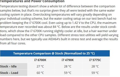
If they're still using TIM they definitely refined the process. Those XTU temps are very good.

- - - Updated - - -

I would have to guess with the temps we had that it may be solder...? But really not sure. That is just a guess and here is why I say that...: I was sitting at 4.9Ghz and 1.449v and didn't hit 70C. BUT... the voltage difference (1.3v stock to 1.449v) is not as much as the jump from 1.1v to 1.45v I had to use with 4790K.

The FIVR is also gone so that saves a few C there as well... so, in the end, we will have to wait like Dino said. :)

Really? I don't see that from the data presented in the linked article. Especially considering the smaller FAB process and the removal of the voltage regulator.
 

Attachments

  • SkyLakeTemps.JPG
    SkyLakeTemps.JPG
    69.1 KB · Views: 144
Really? I don't see that from the data presented in the linked article. Especially considering the smaller FAB process and the removal of the voltage regulator.
After further reading from another forum, I have heard two things...

1. Its a slightly better TIM
2. The IHS is thinner.

As I said, it was just a guess based on the information I had at the time and the results I personally had. I was several degrees warmer with the 4790K in MY testing. BUt, as you likely know, each CPU is different, so results will vary from CPU to CPU especially considering every test is using two different samples than I am. So comparing my results against anyone else's really isn't applicable/doesn't say anything.
 
Last edited:
- - - Updated - - -


Really? I don't see that from the data presented in the linked article. Especially considering the smaller FAB process and the removal of the voltage regulator.

Correct me if I'm wrong, but doesn't the smaller fab process make it harder to cool??
 
Typically, with a smaller FAB process comes lower voltage. But, (and this is my guess here again), due to the FIVR not being on die, the starting voltage is much higher than with Haswell where most chips started around 1.15v give or take, Skylake is starting out, at least mine and Dino's sample, around 1.3v. I have seen others around 1.24v. So there is that to consider as well.

But I believe you are correct. The more dense something is, the more difficult it is to get the heat out it.

That's what I was thinking. Same TDP, less area, more difficult to cool.
 
So with the voltage regulator now on the motherboard, is that going to present an issue with regard to cooling that component? When it was on the CPU die it got cooled with everything else in the chip.
 
So with the voltage regulator now on the motherboard, is that going to present an issue with regard to cooling that component? When it was on the CPU die it got cooled with everything else in the chip.

When has that ever been an issue for Intel's mainstream platform?
 
It presents the same issues we had with Z77 on down (not much of one at all)... but with intel, not really. Its not like you need a fan blowing on it as you need to in some cases with AMD.

I do believe that at least a little more thought should go into the power areas when overclocking heavily with Skylake. For instance, I wouldn't rock a 4 phase unheatsinked board (if any exist) and overclock skylake.

It wont matter to the majority of people though... except maybe enthusiasts here... (my take.. time will tell if my theories are off)
 
So, the voltage regulation component that has been moved off the CPU die onto the motherboard is not the same as what we call the VRM which lives next to the socket and has mosfets, chokes and capacitors. Correct?
 
So, the voltage regulation component that has been moved off the CPU die onto the motherboard is not the same as what we call the VRM which lives next to the socket and has mosfets, chokes and capacitors. Correct?

It had a new name while on-chip.

FIVR = Fully Integrated Voltage Regulator
VRM = Voltage Regulation Module

Same function, different location.
 
So why on my z97 motherboard do I have a big heatsink just west of the socket? That's not the VRM it's cooling? Sorry, but I'm coming from a long time AMD experience.
 
As I understand it...

Here is how it works on Z97:

The motherboard gets its power from the 12v CPU power lead (that 8 pin typically NW of the processor). That 12v is then stepped down by the VRM's and sent to the FIVR. The FIVR has a typical voltage of around 1.8/1.9 (IIRC). The FIVR then sends even more stepped down voltages to the individual controllers on the CPU die (think PCIe/iGPU etc).

Z170:

12v CPU power input -> VRMs -> CPU.


EDIT: Here is a more technical breakdown of what I said regarding the FIVR from Anand:
The other big part of the Haswell power story is what Intel is calling FIVR: Haswell’s Fully Integrated Voltage Regulator. Through a combination of on-die and on-package circuitry (mostly inductors on-package), Haswell assumes responsibility of distributing voltages to individual blocks and controllers (e.g. PCIe controller, memory controller, processor graphics, etc...). With FIVR, it’s easy to implement tons of voltage rails - which is why Intel doubled the number of internal voltage rails. With more independent voltage rails, there’s more fine grained control over the power delivered to various blocks of Haswell.

Thanks to a relatively high input voltage (on the order of 1.8V), it’s possible to generate quite a bit of current on-package and efficiently distribute power to all areas of the chip. Voltage ramps are 5 - 10x quicker with FIVR than with a traditional on-board voltage regulator implementation.

In order to ensure broad compatibility with memory types, there’s a second input voltage for DRAM as well.
 
So why on my z97 motherboard do I have a big heatsink just west of the socket? That's not the VRM it's cooling? Sorry, but I'm coming from a long time AMD experience.

There's still chokes and other power delivery components, just not the regulation of the actual vCore.
It's stepped down to "CPU Input Voltage" from 12V, then it goes to the FIVR that steps it down to vCore.
 
Back