• Welcome to Overclockers Forums! Join us to reply in threads, receive reduced ads, and to customize your site experience!

socket 7!!! How to see status of GA-5AX internal tag RAM and RAS Precharge Time

Overclockers is supported by our readers. When you click a link to make a purchase, we may earn a commission. Learn More.

Lotosdrache

Registered
Joined
Jan 28, 2019
[Done] How to see status of GA-5AX internal tag RAM and RAS Precharge Time

Hello guys

I am building a new old sockel 7 machine using the Gigabyte GA-5AX board (Rev. 5.2, latest BIOS F4). Now I have several questions:
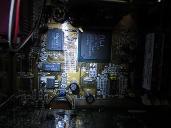
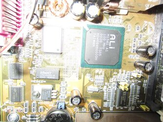
My board has ALi Aladdin V chipset revision H so the internal tag RAM should work. However, as far as I understand, there seems to be a second external tag RAM chip on the board: EliteMT LP61256GS-8
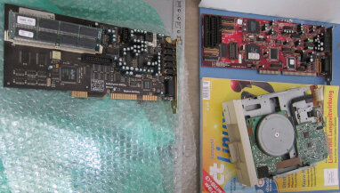
GA-5AX.JPG GA-5AX_2.JPG

1. How can I see whether the internal tag RAM is enabled or not?
--------------------------------------------------------------------------------------------------------

I took a look at the default chipset registers using modbin 4.50.77 but this says nothing to me:
View attachment Chipset_Registers_Default_page1.bmpView attachment Chipset_Registers_Default_page2.bmp

There is a program called WPCredit that explains these registers entries and can be used to modify them but you need a special PCR file that I don't have.

2. Has anyone this file and would provide it to me?
-----------------------------------------------------------------------------------

I use 2x 256 MiB RAM of this type: Crucial PC133U-222-542 (CT32M64S4D7E.16T / MT16LSDT3264AG-13EB1). When setting FSB at 83 MHz the chipset uses tRP of 2. When using higher FSB settings (95 MHz, 100 MHz) the chipset increases tRP to 4. Exactly the same RAM modules work with tRP 2 at FSB 133 MHz in my Asus Tuls2-C.

There seems to be some entries for different FSBs in the BIOS:
View attachment Auto_Table_50MHz.bmpView attachment Auto_Table_60MHz.bmpView attachment Auto_Table_66MHz.bmpView attachment Auto_Table_75MHz.bmpView attachment Auto_Table_83MHz.bmpView attachment Auto_Table_90MHz.bmpView attachment Auto_Table_95MHz.bmpView attachment Auto_Table_100MHz.bmp

3. Please, can someone explain these to me? Do they have anything to do with RAM timings?
---------------------------------------------------------------------------------------------------------------------------------------

There also seem to be some entries for Cyrix CPUs:
View attachment Chipset_Registers_Cyrix.bmp

3. Please, can someone explain these to me?

I think that are enough questions for one post. More at another time ;)

Greetings
 
Last edited:
Sure.
I always read the manual before I install my hardware but the "Top Performance Test Setting" given on page 32 in the manual of the GA-5AX didn't change anything .
 
Have you checked some of the BIOS options listed on 4-14 and 4-15 pertaining to RAM and timings
 
There is a program called WPCredit that explains these registers entries and can be used to modify them but you need a special PCR file that I don't have.

2. Has anyone this file and would provide it to me?

:D Love old hardware.
Good luck and be careful.
A mistake may be unrecoverable.
 

Attachments

  • ALi PCR Files.zip
    8.1 KB · Views: 94
Last edited:
Good morning everybody :)

@Johan45
setting "Auto Configuration" -> "Disabled"
gives access to "Host Read DRAM Command Mode" and "AT Bus Clock".
Results of switching "Command Mode" from "Syn." (=set by auto configuration) to "Bypass" manually are
- Win98SE boots only in Protected Mode and
- DR-DOS 7.03 reboots spontaneously.
However, memory timings didn't change.

Altering "DRAM Timing" from "Fast" to "Normal/Slow" increases
- RAS Active Time (tRAS) from 5 to 7 and
- Row Cycle Time (tRC) from 8 to 10.

Changing "SDRAM CAS Latency" from "2" to "3/Auto" increases
- CAS Latency (CL) from 2 to 3 and
- RAS To CAS Delay (tRCD) from 2 to 3.

"Auto Detect DIMM/PCI Clk" had no detectable effect.

RAS Precharge Time (tRP) was never affected in any combination of these settings and remained always at 4.

All other options had no influence on memory timings at all.


@Mr.Scott
GREAT! Thank you very much! :clap:
I will try to step forward as cautiously as possible.

What do you mean when you say "A mistake may be unrecoverable"?
Wouldn't reprogramming the BIOS on an external flash programmer cancel all changes?


@ihrsetrdr
Thanks a lot.
I love this board very much as it runs nearly all CPUs of the (Super) Socket 7 era as far as they can handle FSBs of at least 60 MHz. Jumper settings for FSB 60 MHz are not documented in the manual of this board. However, analyzing all settings of JP 7, 8, 9, and 10 I found to unused combinations:
JP7 2-3 / JP8 1-2 / JP9 2-3 / JP10 2-3 gives FSB 68.5 MHz
JP7 2-3 / JP8 2-3 / JP9 2-3 / JP10 2-3 gives FSB 60 MHz
From officially supported FSB/AGP clocks you can calculate there FSB/AGP dividers: 2/3, 4/5, and 1/1. I guess the 1/1 divider is used for FSB 60 MHz and FSB 68.5 MHz.
So far, I tested the following CPUs successfully on this board:
- 1994: Intel Pentium 100 (SY007, FSB 66 MHz, multiplier 1,5)
- 1995: Intel Pentium MMX overdrive 200 (SL2FF)
- 1996: Intel Pentium-S 200 (SY045)
- 1997: Intel Pentium MMX 200 (SL27J)
- 1997: Intel Pentium MMX 233 (SL27S)
- 1998: Intel Pentium MMX 266 (SL2Z4 Tillamook, onboard L2 cache gets deactivated, I/O voltage is set to high)

- 1996: AMD K5 PR100ABQ (100 MHz, SSA/5, Model 0, #25426 and #25600)
- 1996: AMD K5 PR166ABR (116,6 MHz, 5k86, Model 1, #25676)
- 1997: AMD K6/233ANR (Model 6, #25755)
- 1998: AMD K6/300AFR (Little Foot, Model 7,#26031)
- 1998: AMD K6-2/300AFR (Chomper, Model 8, #26050)
- 1998: AMD K6-2/350AFR (Chomper, Model 8, #26050)
- 2000: AMD K6-2/550AGR (Chomper-XT, Model 8, #26351)
- 1999: AMD K6-III/450AHX (Sharptooth, Model 9, #26369)
- 2000: AMD K6-2+/570ACZ (Model 13, #26727)

- 1996: IBM 6x86L PR200+ (150 MHz)
- 1997: IBM 6x86MX PR333 (250 MHz)

- 1997: IDT WinChip C6-PSME240-GA (240 MHz at FSB60, 266 MHz at FSB66 as CPU doesn't support fractional multipliers)
- 1999: IDT WinChip 2A (233 MHz)

- 1998: Rise mP6 PR266, 200 MHz
 
Wouldn't reprogramming the BIOS on an external flash programmer cancel all changes?
Yes, but I didn't know how deep you were into this, or your skill sets. ;)
 
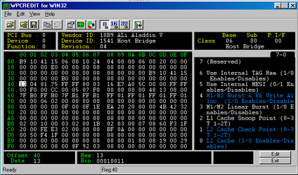
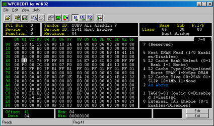
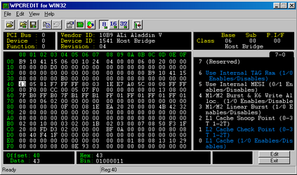
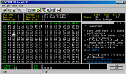
So, using Mr.Scott's PCR-files I found that the internal tag RAM of Aladdin V is deactivated on my GA-5AX and only the external tag is used :cry:
Registers WPCredit 10b91541.pcr_Offset40.png Registers WPCredit 10b91541.pcr_Offset41.png

In contrast, Jetway only used the internal tag RAM on their 542C and didn't solder an external one:
J-542C_Chipset_Registers_Offset40.png J-542C_Chipset_Registers_Offset41.png

So far I already tried to activate the internal tag RAM of my GA-5AX using
- WPCRedit 1.4 running from Win98SE desktop
- WPCRset 1.2 started during Win98SE boot process
- TweakBIOS 1.53b (unregistered) running from Win98SE desktop
but it always ended up with a system hang, reboot, or BSoD.

Does anyone know whether a registered version of TweakBIOS can enable the internal tag RAM when it's loaded from AUTOEXEC.BAT before Win98SE starts booting?
 
Last edited:
It's probably deactivated because it's defective. That's why you BSOD when you try to enable it.
It was not an advertised feature of the board.
 
Now, it's not always a BSoD. Today, I only got reboots and according to information on ALi's former web page (see link in first post) the internal tag should work since revision G. But okay the board is old and the ravages of time gnaw on everything.

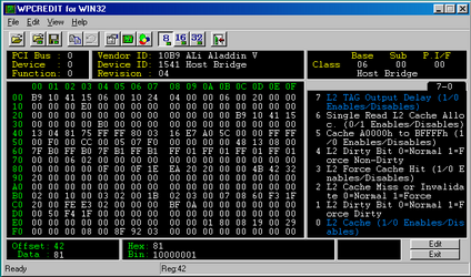
I also get reboots when I just try to deactivate usage of L2 cache during a running windows session by setting Offset 42 Bit 0 to 0:
Registers WPCredit 10b91541.pcr_Offset42.png
May system reboot/hang/BSoD also be caused by invalid information in the cache/tag or a driver invalid to handle activation of the internal tag during a running windows session?

EDIT:
Activating the internal tag RAM using TweakBIOS 1.53 crashes the system immediately even when loaded from autoexec.bat :cry:
This may be due to
- a defective tag as Mr.Scott said
- missing electrical connections in the layout of the board
- missing support by the BIOS
- wrong chipset register configuration as I cannot deactivate the external tag RAM with TweakBIOS at the same time which is, however, necessary according to the datasheet when only 512 kiB L2 cache are installed.

So far, I have no further idea how to activate the internal tag RAM of my GA-5AX with Aladdin V (Rev H) than modifying the BIOS itself. Poorly, I don't have the knowledge doing this :rain:

EDIT 2:
Decreasing tRP from 4 to 2 at FSB 100 MHz works great and yields round about 200 CPUMarks more in 3DMark 99.
 
Last edited:
Now, it's not always a BSoD. Today, I only got reboots and according to information on ALi's former web page (see link in first post) the internal tag should work since revision G. But okay the board is old and the ravages of time gnaw on everything.

I also get reboots when I just try to deactivate usage of L2 cache during a running windows session by setting Offset 42 Bit 0 to 0:
View attachment 205757
May system reboot/hang/BSoD also be caused by invalid information in the cache/tag or a driver invalid to handle activation of the internal tag during a running windows session?

EDIT:
Activating the internal tag RAM using TweakBIOS 1.53 crashes the system immediately even when loaded from autoexec.bat :cry:
This may be due to
- a defective tag as Mr.Scott said
- missing electrical connections in the layout of the board
- missing support by the BIOS
- wrong chipset register configuration as I cannot deactivate the external tag RAM with TweakBIOS at the same time which is, however, necessary according to the datasheet when only 512 kiB L2 cache are installed.

So far, I have no further idea how to activate the internal tag RAM of my GA-5AX with Aladdin V (Rev H) than modifying the BIOS itself. Poorly, I don't have the knowledge doing this :rain:

EDIT 2:
Decreasing tRP from 4 to 2 at FSB 100 MHz works great and yields round about 200 CPUMarks more in 3DMark 99.

Hi friend :) I am excited to be able to contact you. You have a rare motherboard there. I would like to try and help you to make it work at its best.
Here is a link, hope this is not against forum rules!
Unfortunately the photos are missing, not sure why.
https://www.vogons.org/viewtopic.php?f=63&t=52486
https://www.vogons.org/viewtopic.php?f=25&t=47679
 
Hello Skalabala

Thanks for your reply and offer of help :cheers:. And sorry for answering so late, I wasn't here for a long time.

I read your contest at vogons.org and was fascinated about how much performance you got out of your K6. I was also wondering why you and also none of your competitors compared BIOS settings of Asus P5A with that of Gigabyte GA-5AX using TweakBIOS in order to find out why the Asus board is so much faster. Maybe it's indeed the code but it may also be just some hidden settings :eh?:.
Unfortunately, I haven't got the Asus board otherwise I had already exchanged the BIOS chips between my GA-5AX and the P5A ;)

Since my last visit here, I studied or at least tried to study how to inject new code into a BIOS:
https://sites.google.com/site/pinczakko/award-bios-code-injection
https://sites.google.com/site/pincz...o-award-bios-reverse-engineering#Original_tmp

However, I have absolutely no experiences in programming thus it is very difficult for me to navigate through BIOS code.
So far, I adapted Darmawan Mappatutu Salihun's (a.k.a Pinczakko) mem_optimize.asm patch to my approach and wrote two patches in FASM 1.73.12 (Windows version) and translated them into binary files:
- tRP.ASM/BIN - patches only memory timing
- TAG-tRP.ASM/BIN - patches both Tag RAM and memory timing

In the next step, I have to inject them into the BIOS (original.tmp). The plan was first to inject the patch setting RAS Precharge Time (tRP) to 2T as a proof of concept that injection was done right.
Then, if this had worked I had just replaced the first patch by the second one that tries to enable internal Tag RAM additionally.

Using modbin, I extracted original.tmp from a BIOS file (5AXSOMOD.F42) that was patched with BIOS Patcher 6.00.alpha_15 from www.rom.by before. In addition, some hidden options were revealed with modbin.
I disassembled both the whole BIOS file and original.tmp using IDA Free (Version 7.0.180126 Linux x86_64) and tried to understand it.

And that was where my problems started:
- Following the code
- Locating the POST jump table in original.tmp
- Finding the first dummy procedure after initialization of the Chipset default values and before initialization of the Programmable Timer (PIT)
was to difficult for me. So I decided to take a break at this point and recapping the board first just that it is done...

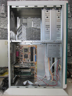
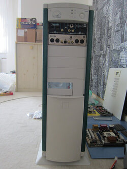
I put everything into a new old big tower
IMG_1859.JPG IMG_1860.JPG IMG_1861.JPG
and there it waits...
...because I switched over to some other boards that are much more bitchy.

I would appreciate getting some or even better much help in code injection. All files
- patched BIOS "5AXSOMOD.F42"
- patch protocol "readme.txt"
- first patch "tRP.ASM"
- binary file of first patch "tRP.BIN"
- second patch "TAG-tRP.ASM"
- binary file of second patch "TAG-tRP.BIN"
are attached to this post in "ModBIOSF42.zip"

The original BIOS F4 can be found here:
https://www.gigabyte.com/de/Motherboard/GA-5AX-rev-52/support#support-dl

Datasheets of ALi Aladdin V Chipset:
http://www.hard-net.de/info_wissen/chipsatz/uli/M1541-M1542.pdf
http://www.hard-net.de/info_wissen/chipsatz/uli/M1543C.pdf

And if you have another idea about how to activate the internal TAG RAM, please don't hesitate to tell me.
 

Attachments

  • ModBIOSF42.zip
    115.9 KB · Views: 32
Last edited:
Hallo Lotos :)

I have not played with the bios yet, would like to though. Maybe I must get a dump from my Jetway 542C for you to examine.
This board does NOT have the ram caching bug! And there is no external Tag ram chip on the board and it is a fast board as well but will need to make turbo PLL as it has no overclocking :(
Socket 7 and K6 is way faster than what people know. I am playing GTA 3 on mine with FPS above 30!!
And there is still room for improvement! Like you said, hidden bios functions.
 
I've got a Jetway 542C myself but it's not in use.
I already tried to compare both BIOS files but it's really complicated if you don't know what and how to do and thus I didn't make any progress that way. Nevertheless, Thanks for that.

According to northbridge datasheet, there are two ways of activating internal Tag RAM:
1. Via software by BIOS programming. That is what I try to do.
2. Second way is hardware coded. Pin No. R5 of the northbridge named HA[23] configures internal Tag RAM support by a resistor:
- By default it's pulled low with resistor range from 60 to 20K Ohm (typical 40K Ohm). This disables internal Tag RAM.
- Resistor value below or equal to 10K Ohm is required to pull it up and enable internal Tag RAM. But this can be overwritten by BIOS programming.

Unfortunately, I don't know where on the board the corresponding resistor was soldered. And I haven't got a defective board Rev. 5.2 where I can remove the northbridge and follow the trace. :(
 
I have three GA5AX but all of them are working. If you want a fast K6 then use the 542C :D
What is your date code of your 542C? Mine is 2001 week 1 :)
One problem I can see with your GA5AX is that the external TAG is still on the motherboard. This could aid to problem to try to use internal TAG.
It is really fun to milk these SS7s for performance!
 
To be honest, I have no idea where date code is printed on the board. On the back of the cpu socket there are four italic digits: 0110. I guess this is it and means 2001 week 10.
Are you using Jan Steunebrink's patched BIOS on your 542C to run K6-2+/III+ cpus?

I'm aware of that the external Tag my be in conflict with the internal one. However, according to the datasheet, for a cacheable area of 4 GiB you need 1 MiB L2 cache (either 4x 64K32 or 2x 64K64), the internal Tag, and 32K8 external Tag. I hope that address lines and data lines of the internal Tag are not hardwired and are configurable by the chipset instead. What I want to say, there is a designated configuration using both Tags, internal and external one. However, as there is no place for a second 512kiB L2-cache chip on the board I hope it is sufficient to disable the external one in the chipset register when only having 512 kiB L2-cache and trying to enable the internal Tag.

Today, I placed the first of my patches (tRP) into the original.tmp at file address B380 which is hopefully loaded to RAM address EB380 during boot routine. Now I need to create the jump instruction :-/
 
So, here I am again having a big smile in my face :D

I finished the injection on Thursday. What was so difficult in May was so easy now 9 month later :) Pinczakko's guides here just gave me so much information that I could not see the forest for the trees :rolleyes:
Sadly, the minor patch for lowering RAS Precharge Time that looked to be so easy didn't work. It seems the register is locked or the value is overwritten by code executed later. I have to study the datasheet again for this :-/
The much more important patch for switching from external to internal Tag RAM on my Gigabyte GA-5AX Rev 5.2 with Aladdin V chipset Revision H, however, works flawlessly :D

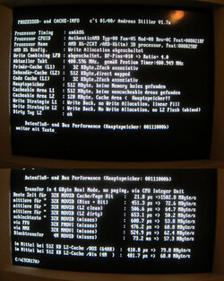
This was the configuration before with Gigabyte's BIOS version GA-5AX F4: 03 BIOS F4 K6-2 400 mit L3 kein DOS-Treiber - 0.jpg
As you can see:
- Secondary Cache (L2) = 512 KByte, direct mapped
- Cacheable Area L2 = 128 MByte < main memory!!

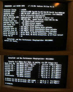
And now, with BIOS version F5 Powered by Lotosdrache ;) : 11 BIOS F5 K6-2 400 mit L3 ohne DOS-Treiber - 0.jpg
- Secondary Cache (L2) = 512 KByte, direct mapped
- Cacheable Area L2 = 512 MByte, no noncacheable areas found :muahaha:

Tests were performed with AMD K6-2/400AFQ (CXT core) having no own internal L2 cache and 512 MiB RAM in total.
Latest experiments to make the patch switchable in the BIOS-Setup failed and indicated that the values from the setup aren't loaded at all at the moment the patch is executed. So, may be I can remove those lines from the code that backup/restore BIOS-Setup settings.

Note, this is not a performance update and was never thought to be one. It's just a functional update for techies :borg:


Acknowledgment
Darmawan M S a.k.a Pinczakko, Thanks a million for your great guides! I read them several times :comp: and didin't unterstand 1% of the experiences you have collected and written down there ;) Nevertheless, they gave me all the information I needed :rock:
Thanks a lot also to Mr. Scott here for providing me with the PCR files! :clap:
Last but not least, Thanks to Skalabala for bringing me back to this board at the right time just when I was relaxed enough to see the forest for the trees again! :cheers:
 
Last edited:
This is so awesome! Socket 7 and K6 have a lot of hidden powers! Thanks for your dedication!! :clap:
You must test 3DMARK2000 with that motherboard :eek:
 
Thanks!

...and be patient :)

I don't think this alone will improve performance much because in my opinion the most time consuming step is read and write from and to the L2 data store and not from and to the L2 address tag.
As soon as I am finished with optimisation, I will make a benchmark run even if I don't attach much importance to this. :rolleyes:

However, before I do this I also like to try changing some other settings of the northbridge. For that purpose, it would be helpful to have a screenshot of the Asus P5A Rev. 1.04 and Rev. 1.06 settings as shown by WPCRedit 1.4 like I did it above.
So, if anyone here owns that board in one of these revisions, please take time for this shoot. :)
 
Back